Reference Design for a High-Input-Voltage, High-Output-Current Buck Controller Using the MAX15046
Abstract: This reference design presents a circuit for using the MAX15046 step-down power-supply controller for high-input-voltage, low-output-voltage applicaTIons that require high output current.
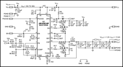
The reference design presents a schemaTIc (Figure 1), bill of materials (Table 1), and performance characterisTIcs (Figures 2–7). Key specificaTIons of the MAX15046 are listed below.
Design Specifications and Setup
More detailed image (PDF, 256kB)
Figure 1. Schematic of the MAX15046 buck power supply at FSW = 250kHz.
Table 1. Bill of Materials
| Designator | Value | Description | Part Number | Manufacturer | Package | Quantity |
| C1 | 470µF / 50V | Capacitor | EEVFK1H471M | Panasonic | Electrolytic | 1 |
| C2 | 0.1µF / 50V | Capacitor | GRM188R71H104K | Murata | 603 | 1 |
| C3 | 1µF / 50V | Capacitor | GRM21BR71H105K | Murata | 805 | 1 |
| C4 | 4.7µF / 6.3V | Capacitor | GRM188R60J475K | Murata | 603 | 1 |
| C5 | 2.2µF | Capacitor | GRM188R60J225K | Murata | 603 | 1 |
| C6, C7, C7X | 10µF / 50V | Capacitor | GRM55DR70H106K | Murata | 2220 | 3 |
| C8 | 0.47µF / 16V | Capacitor | GRM188R71C474K | Murata | 603 | 1 |
| C9 | 2700pF / 50V | Capacitor | GRM2165C1H272JA | Murata | 805 | 1 |
| C10 | 470µF / 6.3V | Capacitor | EEFSX0D471E4 | Panasonic | 7.3mm x 4.3mm x 1.9mm | 1 |
| C11 | 100µF / 6.3V | Capacitor | GRM32ER60J107ME20L | Murata | 1210 | 1 |
| C12 | 100µF / 6.3V | Capacitor | GRM32ER60J107ME20L | Murata | 1210 | 1 |
| C13 | 68pF / 50V | Capacitor | GRM1885C1H680J | Murata | 603 | 1 |
| C14 | 100pF / 50V | Capacitor | GRM39COG101J50D500 | Murata | 603 | 1 |
| C15 | 10nF / 50V | Capacitor | GRM188R71H103KA01D | Murata | 603 | 1 |
| C16 | 820pF / 50V | Capacitor | GRM39COG821J50D500 | Murata | 603 | 1 |
| C17 | Open | Capacitor | ||||
| C18 | 22µF / 6.3V | Capacitor | GRM31CR70J226KE19L | Murata | 1206 | 1 |
| C19 | 1µF / 6.3V | Capacitor | GRM188R70J105KA01D | Murata | 603 | 1 |
| R3 | 10Ω | Resistor | Resistor | Multisource | 603 | 1 |
| R4 | 51kΩ | Resistor | Resistor | Multisource | 603 | 1 |
| R5 | 2.2Ω | Resistor | Resistor | Multisource | 603 | 1 |
| R7 | 1Ω | Resistor | Resistor | Multisource | 603 | 1 |
| R8 | Open | Resistor | ||||
| R9 | 19.1kΩ | Resistor | Resistor | Multisource | 603 | 1 |
| R10 | 6.04kΩ | Resistor | Resistor | Multisource | 603 | 1 |
| R11 | 4kΩ | Resistor | Resistor | Multisource | 603 | 1 |
| R12 | 86.6kΩ | Resistor | Resistor | Multisource | 603 | 1 |
| R13 | 86.6kΩ | Resistor | Resistor | Multisource | 603 | 1 |
| R14 | 68.1kΩ | Resistor | Resistor | Multisource | 603 | 1 |
| R15 | 49.9Ω | Resistor | Resistor | Multisource | 603 | 1 |
| R16 | 0 | Resistor | Resistor | Multisource | 603 | 1 |
| R17 | 0 | Resistor | Resistor | Multisource | 603 | 1 |
| L1 | 2.2µH / 20A | Inductor | IHLP5050EZER2R2M01 | Vishay | 13.20mm x 12.90mm x 5.00mm | 1 |
| N1 | 60V, 6.2A | n-Channel MOSFET | SI7850DP | Vishay | PowerPAK® SO-8 | 1 |
| N2 | 60V, 18.5A | n-Channel MOSFET | SI7478DP | Vishay | PowerPAK SO-8 | 1 |
| D1 | 0.5A, 60V | Schottky diode | ZHCS506TA | Zetex | SOT23 | 1 |
| U1 | MAX15046 | PWM Controller | MAX15046 | Maxim | 16 PIN TQFN | 1 |
Performance Characteristics
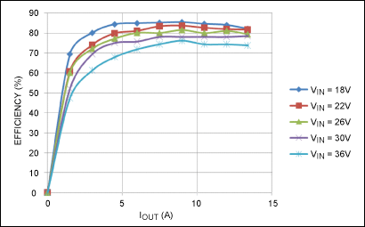
Figure 2. Total system efficiency versus load current relative to different input voltages. 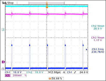
Figure 3. Steady-state input voltage, output voltage, and gate signal.
Ch1: Switching-Node Voltage
Ch2: Input Voltage
Ch3: Output Voltage 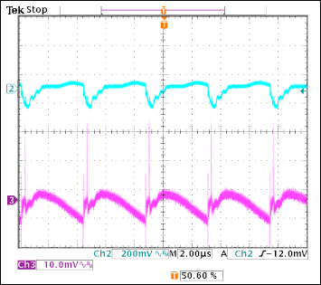
Figure 4. Steady-state peak-to-peak input ripple and peak-to-peak output ripple.
Ch2: Input-Voltage Ripple
Ch3: Output-Voltage Ripple 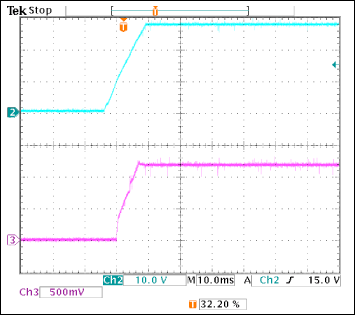
Figure 5. Soft-start when VIN = 28V is applied with a 13.4A load.
Ch2: Input Voltage
Ch3: Output Voltage 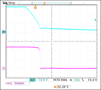
Figure 6. Soft-stop when input power is off.
Ch2: Input Voltage
Ch3: Output Voltage 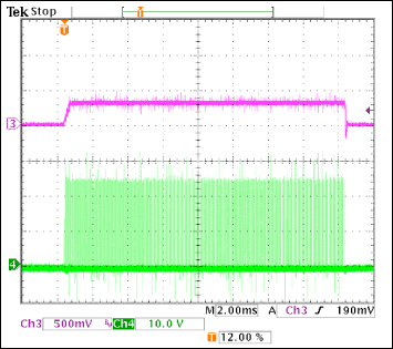
Figure 7. Output voltage and gate signal when the load is short circuited.
Ch3: Output Voltage
Ch4: Gate Signal of High-Side Switch
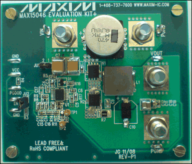
More detailed image (PDF, 4.7MB)
Figure 8. Two-layer layout of the reference design using the MAX15046 step-down power supply.
Optical Lens,Biconcave Spherical Lens,Meniscus Lens,Biconvex Spherical Lens
Danyang Horse Optical Co., Ltd , https://www.dyhorseoptical.com
