
A chopper circuit (also known as a DC chopper circuit) means that a portion of a sine wave is "cracked off" for some purpose in power operation.
(For example, when the voltage is 50V, the electronic component is used to cut off the 50~0V part, and the output voltage is 0.) Later, it is borrowed from the DC-DC switching power supply, mainly in the process of voltage regulation of the switching power supply. The power supply is “pulled†by the line. Convert DC power to another fixed voltage or adjustable voltage DC. Also known as DC-DC converter.
Duty cycleIt refers to the ratio of the energization time to the total time in one pulse cycle. The duty ratio (Duty Ratio) has the following meanings in the field of telecommunications: for example, a pulse width of 1 μs and a pulse sequence duty cycle of 0.25 for a signal period of 4 μs.
The duty cycle is the percentage of time the circuit is turned on as a percentage of the total circuit duty cycle. For example, if a circuit is turned on halfway through one of its duty cycles, its duty cycle is 50%. If the signal voltage applied to the working element is 5V, the actual operating voltage average or voltage effective value is 2.5V. Assume that the component is an electronic valve. When the circuit is fully turned on, the valve is fully open; when the duty cycle is 50%, the valve state is half open. Similarly, when the duty cycle is set to 20%, the valve opening should obviously be 20%. In this way, the valve can be arbitrarily adjusted from 0% (fully closed) to 100% (fully open).
Chopper circuit control methodFixed frequency modulation pulse width, fixed pulse width modulation frequency, frequency modulation and widening
The circuit characteristics are represented from the perspective of the duty cycle. By calculating the respective voltage, current and power relationships in the circuit, the duty cycle is used to represent the size range and extreme values ​​of these elements, and the circuit performance of each electronic device is compared and analyzed from the perspective of the duty cycle.
1, step-down chopper circuitThe buck chopper circuit, also known as the Buck chopper circuit, is characterized by an output voltage that is lower than the input voltage and an output current that is higher than the input current. That is, the conversion of the circuit can convert the DC power supply voltage to an output DC voltage lower than its value, and realize the conversion of electric energy.
In Figure 1, T is a switching device, which can select different power electronic devices according to the application requirements; L and C are filter inductors and capacitors to form a low-pass filter; R is a load; VD is an iL freewheeling diode. When T is disconnected, VD provides a freewheeling path; E is the input DC voltage; U0 is the average of the output voltage. When IGBT is selected as the switching device, the circuit is shown in Figure 1.
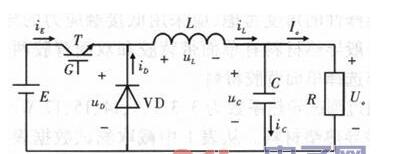
Figure 1 Buck circuit structure diagram
According to the continuous condition of the inductor current in the circuit, the step-down chopper circuit can be divided into two modes: continuous conduction and discontinuous conduction. In this paper, Ts is the conduction period.
1.1, inductor current continuous conduction mode
The continuous conduction mode corresponds to the case where the inductor current is constant “0â€. Let the control signal of the switching device T be UG. When UG is high, T is turned on, and when UG is low, T is turned off.
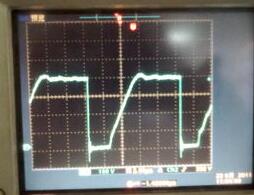
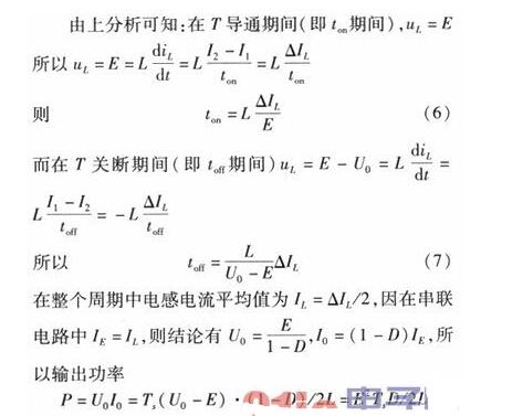
The working principle of the circuit is: set the circuit to be in a stable working state. When t=0, the T is turned on. Because the diode VD is reverse biased, the voltage across the inductor is uL=E-U0, and is positive. At this time, the power source E transmits energy to the load through the inductor L, and the current iL in the inductor linearly increases from I1 to I2, and the energy storage increases. At t=ton time, T is turned off, and iL cannot be abrupt, so iL will continue to flow through diode VD, L energy storage is consumed on load R, iL linearly attenuates, and energy storage decreases. When uL=-U0, due to the unidirectional conductivity of VD, iL can only flow in one direction, that is, there is always iL ≥ 0, so that a unipolar DC voltage is obtained on the load R. Select the appropriate value of the inductor and capacitor, and control T to periodically switch, you can control the average value of the output voltage and make the output voltage ripple within the allowable range. Obviously, the longer the T conduction time, the more energy is transferred to the load and the higher the output voltage. The working waveform when T is turned on and off is shown in Figure 2.
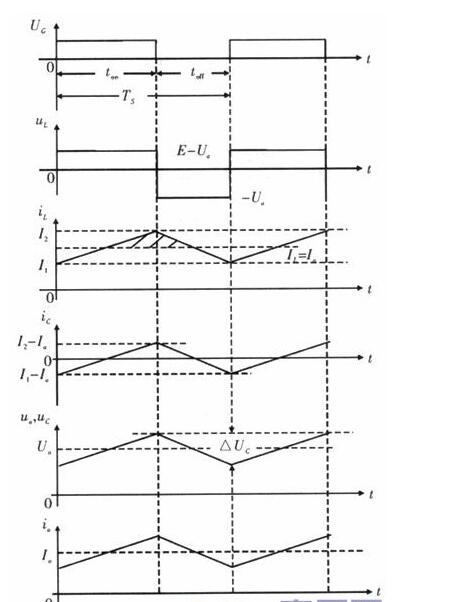
Figure 2 Step-down chopper circuit working waveform
It can be seen from Fig. 2 that the power supply current exists only during the period of T conduction, and the circuit is already in a stable working state. When t=0, the T is turned on, and the diode VD is reverse biased, so the voltage is UL, uL = E-U0 and is positive. At this time, the power source E transmits energy to the load through the inductor L, and the current iL in the inductor linearly increases from I1 to I2 (ie, ie=iL), and the energy storage increases.
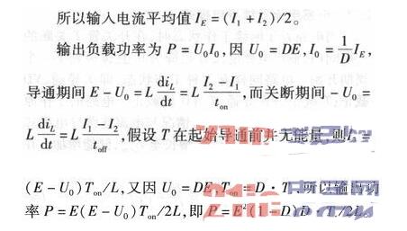
According to the function curve of the output power, P is the largest when D=0.5, so that the power range after the step-down of the load terminal can be calculated from 0 to E2Ts/8L, thereby providing the user with a better voltage power parameter.
1.2, inductor current interrupt mode
In the entire switching period Ts of the inductor current continuous conduction mode, the inductor current iL is "0" and varies between I1 and I2. The inductor current intermittent conduction mode means that the inductor current iL has dropped to 0 during the toff period during which the switching device T is turned off, and is kept for a certain time, and the circuit has three operating states, that is, T is turned on, VD is turned off; T is turned off, VD is turned on. Both T and VD are cut off, and the inductor current is zero. The working principle of the circuit is: when T=0, the T is turned on, the situation is the same as the continuous current conduction mode, the current iL in the inductor linearly increases to ILmax, and the energy storage increases. At time t = ton, T is turned off and iL continues to flow through the diode VD. However, before the next conduction period of T, iL has decayed to 0, and the freewheeling diode VD is also turned off. When both T and VD are off, the voltage and current waveforms of the interrupted conduction mode of the inductor current are as shown in FIG.
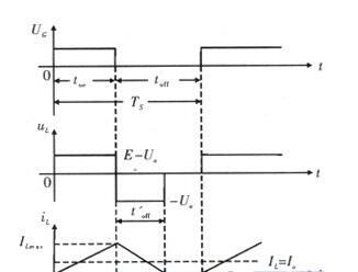
Figure 3 voltage and current waveform
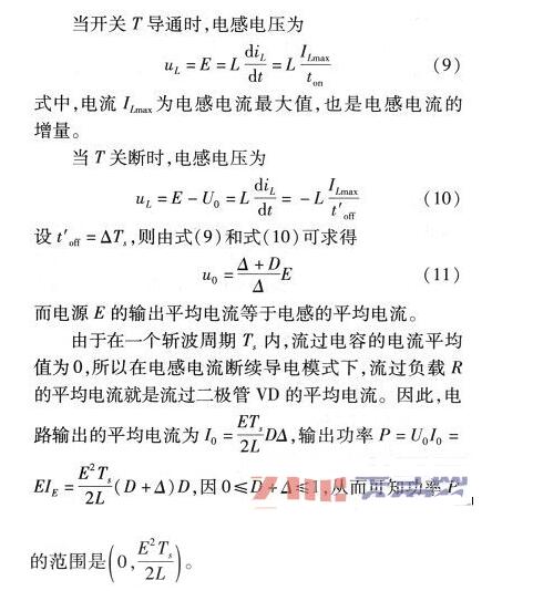
When T is turned on, the inductor voltage is
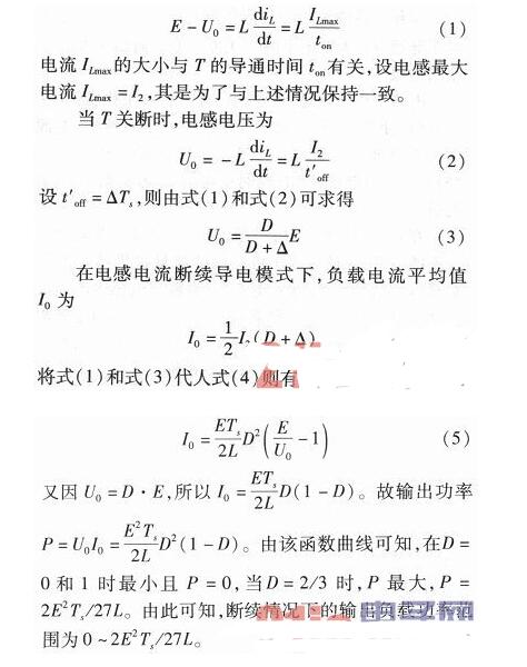
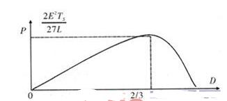
Figure 4: Output power and space ratio curve at the time of discontinuity
2. Boost chopper circuitFigure 5 is a boost chopper circuit. Also known as the Boost chopper circuit, which is used to convert the DC power supply voltage to a DC output voltage higher than its value, thereby realizing the transfer of energy from the low-voltage side power supply to the high-voltage side load.
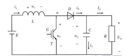
Figure 5: The structure of the boost chopper circuit
2.1, inductor current continuous conduction mode
Let the control signal of the switching device T be UG. When UG is high, T is turned on, and when UG is low, T is turned off. The T turn-on and turn-off are similar to the buck map.
The working principle of the circuit is: set the circuit to be in a stable working state. When t=0, the T is turned on, the diode VD is subjected to the back pressure and cut off, the power supply voltage E is all added to the inductor L, and the current iL in the inductor linearly increases from I1. To I2, and the energy storage increases; at the same time, the capacitor C supplies energy to the load R.
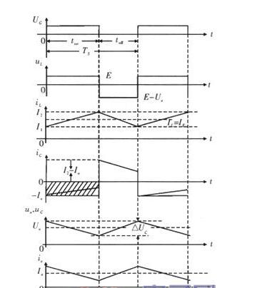
Figure 6 Working waveform of the boost chopper circuit
At t=ton, UG is low and T is turned off. Because the inductor current cannot be abrupt, iL supplies the stored energy to the capacitor and load through VD, that is, the energy storage of the inductor is transmitted to the capacitor and load side. The current iL in the inductor is linearly reduced from I2 to I1, and the stored energy is reduced. The induced potential generated by the inductor prevents the current from decreasing, and the induced potential is UL0, so U0"E. The working waveform of each electric quantity under T conduction and shutdown conditions is shown in Fig. 6.
From the output power expression, it can be seen that the output power is ideally equal to the input power, and the output power is proportional to the duty cycle. In the same case, the larger the duty cycle, the larger the output power, and the output power range is 0~E2Ts/ 2L.
2.2, inductor current intermittent conduction mode
When the circuit is in the intermittent operation state, during the toff period during which the switching transistor T is turned off, the output inductor current iL has dropped to 0, and is held until the next cycle begins. The circuit also has three working states, that is, T is turned on, VD is turned off; T is turned off, VD is turned on; T and VD are all cut off. The working principle of the circuit is: when T=0, the T is turned on, the situation is the same as the continuous current conduction mode, the current iL in the inductor linearly increases to ILmax, and the energy storage increases. At time t = ton, T is turned off and iL simultaneously charges capacitor C and energizes load R through diode VD. But the next conduction cycle at T
Before the arrival, iL has decayed to 0, so that the current is intermittent. At this time, both T and VD are cut off. Its voltage and current waveforms are shown in Figure 7.
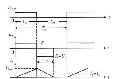
Figure 7 Intermittent state voltage and current waveform diagram
The principle of the buck-boost chopper circuit is introduced. By calculating the voltage, current and power range of the circuit from the angle of duty cycle, the influence of the duty cycle on the performance of the circuit power can be found, thus embodying the duty cycle in the circuit. The optimal control of each performance, and the selection of a suitable duty cycle for a specific circuit to some extent, that is, the optimal control of the circuit, which is equivalent to the output effect of the amplifier circuit to optimize the output function. This is only to study the optimization of device performance from a single perspective, and there are still many device optimization problems to be solved. It is expected that with the research and development of power devices, its performance will continue to increase, which will result in better new devices, which provides users with more choices when selecting power electronics.
Liquid Crystal Display For Medical Use
Liquid Crystal Display For Medical Use,Super Liquid Crystal Instrument Medical Display,Medical Liquid Crystal Instrument Lcd Display,Thin Transparent Lcd Medical Display
Dongguan Yijia Optoelectronics Co., Ltd. , https://www.everbestlcdlcms.com