LED (Light-emitting diode) is widely used in the fields of indication and display due to its advantages of long life and low energy consumption. Reliability, stability and high light extraction rate are factors that must be considered when LEDs replace existing lighting sources. The packaging process is one of the main factors that affect the function of the LED. The key processes of the packaging process include rack mounting, pressure welding, and packaging. Due to the packaging process itself, there are many defects in the LED packaging process (such as repeated soldering, chip electrode oxidation, etc.). Statistics show that the failure of the soldering system accounts for 25% to 30% of the entire semiconductor failure mode. [3] Due to the dual limitations of equipment and output, most manufacturers use manual welding, and the unqualified welding system accounts for more than 40% of the total number of unqualified. From the perspective of use, although the defects generated in the LED packaging process do not affect its photoelectric performance at the initial stage of use, they will gradually be exposed and cause device failure in the subsequent use process. In some application areas of LEDs, such as high-precision aerospace equipment, the potential defects are more harmful than those that cause immediate fatal failure. Therefore, how to realize the detection of LED chips during the packaging process and block defective LEDs from entering the subsequent packaging process, thereby reducing production costs, improving product quality, and avoiding the use of defective LEDs to cause major losses has become the LED packaging industry. Problems that need to be solved urgently.
At present, the inspection technology of the LED industry mainly focuses on the wafer-level inspection before packaging [4-5] and the finished product-level inspection after the packaging is completed, while the domestic inspection technology for LEDs in the packaging process is not yet mature. Based on the non-contact detection method of LED chips, this paper uses the pn junction photovoltaic effect in the LED pin-type packaging process to analyze the impact of packaging defects on the loop photocurrent generated by the light irradiated LED chip in the lead frame. The law of electromagnetic induction measures the photocurrent of this loop to realize the detection of chip quality and packaging defects in the LED packaging process.
1 Theoretical analysis1.1 Photovoltaic effect of pn junction [m] According to the photovoltaic effect of pn junction, the photocurrent IL is expressed as:

In the formula, A is the area of ​​the pn junction, q is the charge of electrons, Ln and Lp are the diffusion lengths of electrons and holes, respectively, J is the average light intensity calculated by the number of photons, α is the absorption coefficient of the pn junction material, and β is the quantum Yield, that is, the number of pairs of electrons and holes per photon absorbed.
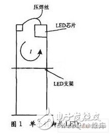
In the LED pin-type packaging process, each LED chip is fixed on the lead frame, and the LED chip forms a closed loop with the lead frame by bonding gold wire (aluminum wire), as shown in Figure 1. If the resistance of the lead bracket is neglected, the photocurrent of the LED bracket loop is equal to the chip photocurrent IL. It can be seen that when the pn junction material and doping concentration are constant, the photocurrent of the stent loop is proportional to the light intensity I.
1.2 Package defect mechanism
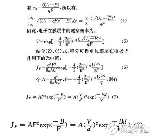
When the LED chip is affected by corrosive factors or contaminated with oil, a non-metallic film is formed on the surface of the chip electrode, resulting in packaging defects. After the pressure welding process of the LED chip with a non-metal film layer on the electrode surface, a metal-dielectric-metal structure is formed at the welding place, which is also called a tunnel junction. When a certain intensity of light is irradiated on the LED chip, if the LED chip fails, no photocurrent flows through the bracket circuit. If the non-metal film layer is thick enough, only a few electrons can tunnel through the barrier of the film layer, and there is no photocurrent flow in the LED bracket circuit. Over; If the non-metal film layer is thinner, since the photo-generated current of the LED chip forms an electric field on both sides of the tunnel junction, electrons mainly tunnel through the film layer in the form of field emission, and the current flowing through the film layer per unit area can be expressed as

Among them, q is the electron power, m is the electron mass, and chu is the Planck constant, vx, vy, and vz are the electron tunneling speeds in the x, y, and z directions, respectively, and T(x) is the electron tunneling probability. And the electron tunneling probability of any barrier can be expressed as

Among them, jin and jout are the current densities entering and passing through the film respectively, and the direction of x is from the surface of the chip electrode to the bonding point, which is the potential barrier at any point in the z direction of the film, and E is the surface velocity of the vertical chip electrode, which is vx The energy of electrons.
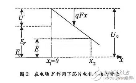
Figure 2 is a diagram of the potential barrier on the surface of the F chip electrode under the action of the electric field f', where EF is the Fermi level and U is the electron emission barrier. From Figure 2, if the chip electrode surface is an abrupt junction, its value is U0, the electric field intensity formed by the photo-generated current on both sides of the tunnel junction is F, and the potential barrier outside the electrode surface is U0-qFx. Take the bottom of the chip electrode conduction band as the reference energy level E0 (x=0), so there are x0 locations, U(x)=U0- qFx, according to the condition U(x)=E=U0- qFx2 where d is the thickness of the film , V is the voltage on both sides of the tunnel junction of the film. When the photovoltaic effect of the LED chip occurs, it can be seen from formula (7) that the current flowing through the non-metallic film on the surface of the chip electrode is affected by the thickness of the film. As the film thickens, the current flowing through the film decreases. The photocurrent flowing through the LED bracket circuit will also decrease.
In summary, the presence or size of the photocurrent of the leaded LED bracket loop can reflect the functional status of the LED chip in the packaging process and the electrical connection between the chip electrode and the lead bracket. Therefore, it can be achieved by detecting the photocurrent of the LED bracket loop Detect chip function status and package defects in the lead-type packaging process.
1.3 Detection method of packaging defects
After the pressure welding process is completed, the LED is in a closed short-circuit state, and it is not feasible to directly export the loop current for detection. Although the stent loop has a certain resistance, the photocurrent is only in the order of microamperes, so the voltage drop in the stent loop is very small, and it is difficult to use general voltage measurement methods, and contact detection will introduce contact resistance, which affects the accuracy of detection . Therefore, consider using a non-contact current detection method. According to Faraday’s law of electromagnetic induction, using the characteristics of the pin-type LED, one end of the magnetic core of the coil with magnetic core is inserted into the closed circuit z shown in Figure 1 during detection. The LED bracket circuit is used as the primary winding, and the coil with magnetic core is used as the secondary winding. A stage winding, and a capacitor C is connected in parallel at both ends of the coil to form an LC resonant circuit with the coil L. When the LED chip is excited by alternating light, an alternating current is generated in the stent loop, and the alternating current-carrying loop generates an alternating magnetic field in the surrounding space, and the alternating magnetic field of the secondary coil generates an induced electromotive force in the secondary coil. If the frequency of the alternating light is equal to the frequency of the LC resonant circuit, the LC circuit resonates, and at this time the induced electromotive force at both ends of the secondary coil is the largest. Therefore, the purpose of detecting the photocurrent of the stent loop can be achieved indirectly by detecting the induced electromotive force at both ends of the secondary coil, and the detection of the chip function status and welding quality in the packaging process can be achieved.
In the LC resonance circuit, the magnetic core in the coil plays a role in enhancing the magnetic induction intensity B, thereby increasing the amplitude of the detection signal. In addition, the relationship between the effective permeability and the relative permeability of the magnetic core in the coil can be expressed as:

In the formula, the effective permeability of the μe magnetic core is the relative permeability of the magnetic core, and μr is the effective magnetic circuit length of the magnetic core, which is called the non-closed air gap length.
It can be seen from equation (8) that the parameters that affect the effective permeability and thus the magnetic induction intensity B are:
â‘ The relative permeability of the magnetic core material. It is related to the selected soft magnetic core material (the initial relative permeability of the soft magnetic material is generally greater than 1000). When the core material is selected, its relative permeability is a certain value.
â‘¡ The effective length le of the magnetic core and the length of the non-closed air gap lg are determined by the structure of the magnetic core. The magnetic field generated by the weak current is susceptible to interference from external factors. The longer the magnetic circuit, the greater the interference, so the effective length of the magnetic core should be short.
When the material of the magnetic core is determined, in order to obtain a larger magnetic induction intensity B, the structure of the magnetic core in the coil needs to be changed. If the magnetic core structure is designed to be ring-shaped, it is known from equation (8) that the increase in magnetic flux density B is theoretically equal to the relative permeability of the magnetic core, and the detection signal amplitude will reach the maximum. A strip-shaped magnetic core is overlapped with a U-shaped magnetic core of the same material as the strip-shaped magnetic core to form a toroidal core coil. There are two ways to overlap, as shown in Figure 3.
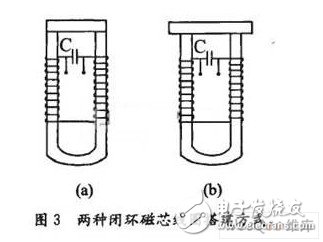
When testing, insert one end of the U-shaped magnetic core with the coil into the closed loop shown in Figure 1, to sense the alternating magnetic flux generated by the loop current in the LED bracket loop, and then lap the strip-shaped magnetic core on the U-shaped magnetic core To close the inductive magnetic circuit. Due to the different overlapping methods, when the magnetic core coils of the two overlapping methods are in the alternating magnetic field generated by the stent loop, the magnetic circuits at the overlapping positions will also be different. Use Ansoft MaxwELl software to simulate the magnetic fields of the two overlapping methods. The magnetic circuit where the core overlap is in an alternating magnetic field, the result is shown in Figure 4

The simulation results of (a) and (b) in Fig. 4 correspond to the two ways of overlapping coil cores in Fig. 3 (a) and (b). Comparing the simulation results of the magnetic circuit at the overlap of the two coils, it can be seen: â‘ Figure 3(a) shows that the magnetic circuit at the overlap of the magnetic core has the shortest loop in the air medium, and the magnetic resistance is the smallest, so the magnetic loss is also the smallest. . â‘¡As the current of the LED stent under test is on the order of microamperes, the excited magnetic field is small, and it is susceptible to the interference of the space electromagnetic field. Figure 3(b) shows that the magnetic circuit at the overlap of the magnetic core is more exposed to the air medium. The probability of interference is greater. From the above analysis, Figure 3(a) has a better magnetic core overlap method, which can enhance the interference suppression capability of the signal detection end, increase the detection signal amplitude, and improve the signal-to-noise ratio of the optically excited detection signal to a certain extent, thereby improving the defect detection accuracy.
2 Experiment and analysis2.1 Experiment
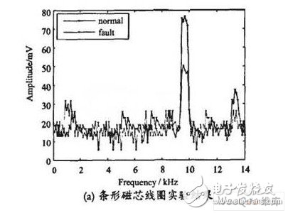
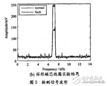
In order to compare the influence of the strip core coil and the toroidal core coil on the inspection accuracy of the package defect, the strip core coil and the toroidal core coil shown in Figure 3(a) are used for experiments. The core material is PC40, its initial relative permeability is about 2300, the strip-shaped core has a geometrical size of 1.6minx3.2ram×20mm, and the number of coil turns is 300; the cross-sectional size of the toroidal core is 1.6mm×3.2 mm, the effective magnetic path length is approximately equal to the strip-shaped magnetic core, and the number of turns of the coil is 300 turns. In the experiment, the excitation light source is a super-brightness SMD white LED. The excitation light source is driven by a square wave signal with a duty cycle of 50%. The square wave signal can be superimposed by a series of sinusoidal signals, so that the fundamental frequency and The working frequency of the resonant circuit is the same, that is, the LC resonant circuit realizes the frequency selection of the square wave signal, so the rate of change of the magnetic flux chain passing through the coil is the rate of change of the square wave fundamental frequency signal; the detection object is GaP material 12mil$ welding quality Qualified LEDs and LEDs with non-metallic films on chip electrodes during soldering. The signal output from both ends of the coil is amplified, filtered, and peak-detected, as shown in Figure 5. The magnification of the amplifier in the experiment is 103 times.
2.2 Result analysis
The LED chip package defect detection method introduced in this article is indirectly realized by detecting the photocurrent of the LED bracket loop. It can be seen from Figure 5 that the magnetic field excited by the photocurrent of the stent loop induces different electromotive forces at both ends of the coils with different core structures; the signal-to-noise ratio of the detection signals varies greatly with coils with different core structures. The specific performance is:
①For LEDs with qualified welding quality, the experimental detection value is consistent with the theoretical calculation value. Figure 5(a) shows the experimental results of using a strip coil core. In the packaging process, when welding qualified LEDs, the optical excitation signal generated by the signal detection end is amplified, filtered, and peak-detected, and the amplitude is about 60mV. Select 12mil$LED chip for theoretical calculation, chip area A=0.3mm×0.3mm, take β=0.5. When the average light intensity per unit area absorbed by semiconductor material in unit time (in terms of photons) is 5.45×10²¹ pieces/ At m2s, the photo-generated current can be calculated from equation (1) to be about 42μA. According to Biot-Savart theorem, superposition theorem and Faraday's law of electromagnetic induction, it can be found that the amplitude of the induced electromotive force of the 12mil$LED chip at the signal detection end is about 63mV, and the experimental error and calculation error are eliminated. The theoretical value and the experimental value are more It fits well.
②For the toroidal core coil, the experimental value is smaller than the theoretical value. According to formula (8), for the strip structure magnetic core coil, assuming that the effective magnetic path length of the magnetic core le=100lg, the effective permeability μe≈100 at this time. If the magnetic core is changed to a ring shape, the length of the non-closed air gap is lg≈0, and the effective permeability μe≈μr=2300 at this time. According to theoretical calculations, the 12mil$ welding quality qualified LED induces an electromotive force amplitude at the signal detection end of about It is 1.4V; from Figure 5(b), the experimental signal value is about 220mV, and the experimental value is much smaller than the theoretical value. The above calculation is carried out under ideal conditions. In the actual experiment process, the toroidal core coil is formed by overlapping the U-shaped magnetic core and the strip-shaped magnetic core. The air gap lg at the overlap still exists, so the magnetic circuit is not It may be completely closed. According to formula (8), the air gap has a great influence on the effective permeability, so the effective permeability is still smaller than the relative permeability. Therefore, the experimental value is much smaller than the theoretical value.
③Different core structures can realize the detection of LED package defects, but the signal-to-noise ratio of the detection signal is quite different. It can be seen from Figure 5 that although the magnetic core coil in the experiment has a different structure, the light excitation detection signal of the LED with qualified welding quality is significantly greater than that of the LED light excitation detection signal with a non-metallic film on the chip electrode surface during the packaging process. By comparing the magnitude of the detection signal amplitude between the two, the LED with non-metallic film on the chip electrode surface can be picked out during the packaging process. For Fig. 5(a), the magnetic core of the coil used in the experiment is a strip structure, there is an air gap lg, the magnetic induction intensity B is enhanced by the effective permeability μe, and the detection signal is susceptible to external interference, so the amplitude of the detection signal is relatively high. The small and large detection noise makes the signal-to-noise ratio of the optical excitation signal of the two chips small, which brings difficulty to the back-end signal processing and affects the accuracy of package defect detection. The magnetic core in the coil is overlapped into a loop to form a closed magnetic circuit, the magnetic induction intensity B is effectively enhanced, the magnetic loss is small, and the interference from the space electromagnetic field is relatively small, so the signal-to-noise ratio of the detection signal is significantly improved.
â‘£Different core structures affect the working frequency of the resonant circuit. During the experiment, the capacitance C of the LC resonant circuit is equal, and the effective permeability of the toroidal core is greater than that of the strip-shaped core. Therefore, the inductance L of the toroidal core coil is greater than that of the strip-shaped core coil. The resonant frequency of the resonant circuit is relatively small; as can be seen from Figure 5, the resonant frequency of the resonant circuit formed by the strip core coil is about 9.75kHz, while the resonant frequency of the resonant circuit formed by the toroidal core coil is about 7.33kHz.
⑤Theoretical analysis and experimental result analysis shows that this method has high detection accuracy for the LED stent loop current. By detecting the magnetic field excited by the stent loop current, the electromotive force is induced at both ends of the coil, and it is compatible with the LEDs with qualified welding quality. The detection signals of the LEDs are compared to realize the detection of LEDs with packaging defects during the packaging process.
3 conclusionAiming at the packaging defects in the process of leaded LED chip packaging, based on the photovoltaic effect of the pn junction, the impact of a packaging defect on the performance of the LED is analyzed by using the electron tunneling effect. Theoretical analysis shows that when there is a non-metal film on the surface of the LED chip electrode, the photocurrent flowing through the LED stent loop is less than the photogenerated current. As the thickness of the film increases, the photocurrent of the loop gradually decreases, and the detection signal decreases. The non-contact method is used to detect the light excitation signal of the LED to be tested and compare it with the qualified LED light excitation signal to realize the detection of the functional status and package defects of the lead-type packaged LED chip during/after the pressure welding process. The factors affecting the detection accuracy are analyzed. The experiment was carried out with a 12mil yellow LED sample with qualified welding and non-metallic film on the surface of the chip electrode. The results show that the method can detect the microampere-level photo-generated current signal of the LED bracket circuit, and has a high signal-to-noise ratio, and the detection result can be achieved. Distinguish the qualified soldering quality from the LEDs with chip failures or packaging defects, so as to achieve the purpose of detecting the functional status of the LED chip during/after the bonding process and packaging defects, thereby reducing LED production costs, improving product quality, and avoiding use. Defective LEDs cause significant losses.
Wireless Charging Power Banks,Fast Charging Wireless Power Bank,Power Banks,Wireless Power Banks
Dongguan Guancheng Precision Plastic Manufacturing Co., Ltd. , https://www.dpowergo.com
