
The current MOS driver has several special requirements
1, low pressure application
When using a 5V power supply, if a conventional totem pole structure is used, since the transistor be has a voltage drop of about 0.7V, the actual voltage finally applied to the gate is only 4.3V. At this time, we use a MOS tube with a nominal gate voltage of 4.5V, which poses certain risks.
The same problem also occurs when using 3V or other low-voltage power supplies.
2. The wide voltage application input voltage is not a fixed value, it will change with time or other factors. This change causes the driving voltage provided by the PWM circuit to the MOS transistor to be unstable.
In order to make the MOS tube safe under the high gate voltage, many MOS tubes have built-in voltage regulators to forcibly limit the amplitude of the gate voltage. In this case, when the supplied driving voltage exceeds the voltage of the regulator, it will cause a large static power consumption.
At the same time, if the gate voltage is simply reduced by the resistor voltage division principle, the MOS transistor will work well when the input voltage is relatively high, and the gate voltage will be insufficient when the input voltage is reduced, causing insufficient conduction, thereby increasing power consumption. .
3, dual voltage applications in some control circuits, the logic part uses a typical 5V or 3.3V digital voltage, while the power part uses 12V or even higher voltage. The two voltages are connected in common ground.
This puts forward a requirement that a circuit needs to be used so that the low-voltage side can effectively control the high-side MOS transistors, and the high-side MOS transistors also face the problems mentioned in 1 and 2 as well.
In these three cases, the totem pole structure can not meet the output requirements, and many off-the-shelf MOS driver ICs do not seem to contain the structure of the gate voltage limit.
So I designed a relatively general circuit to meet these three requirements.
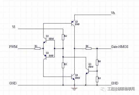

A simple analysis of the NMOS driver circuit:

Vl and Vh are the low-end and high-end power supplies, respectively, and the two voltages can be the same, but Vl should not exceed Vh. Q1 and Q2 form an inverted totem pole to achieve isolation while ensuring that both driver tubes Q3 and Q4 do not conduct at the same time.
R2 and R3 provide the PWM voltage reference. By changing this reference, the circuit can work in the steeper position of the PWM signal waveform.
Q3 and Q4 are used to provide the drive current. Since Q3 and Q4 have a voltage drop of only Vce with respect to both Vh and GND at the time of conduction, this voltage drop is usually only about 0.3V, much lower than Vce of 0.7V. R5 and R6 are feedback resistors used to sample the gate voltage. The sampled voltage has a strong negative feedback to the bases of Q1 and Q2 through Q5, limiting the gate voltage to a finite value. This value can be adjusted by R5 and R6.
Finally, R1 provides the base current limit for Q3 and Q4, and R4 provides the gate current limit for the MOS transistor, which is the limit of Ice for Q3 and Q4. When necessary, the capacitor can be accelerated in parallel with R4.
This circuit provides the following features:
1, using low-end voltage and PWM drive high-end MOS tube.
2. MOS transistors with high gate voltage requirements driven by small amplitude PWM signals.
3, peak limit of gate voltage
4, input and output current limit
5. By using suitable resistors, very low power consumption can be achieved.
6, PWM signal inversion. NMOS doesn't need this feature and can be solved by pre-inverting an inverter.
Low volatge panel distribution system with CCC Certificate:
. Customized low volatge panel
. LV distribution
. MCC system
. Lighting system
. Air conditioner control system
. Fire protection system
Lv Panel,Lv Distribution,Low Voltage Panel,Low Voltage Distribution
Guangdong Superwatt Power Equipment Co., Ltd , https://www.swtgenset.com