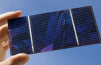
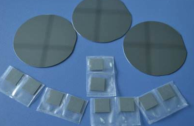
Gallium arsenide is an important semiconductor material. It is a III-V compound semiconductor. It is a sphalerite crystal lattice structure with a lattice constant of 5.65×10⁻¹⁰m, a melting point of 1237°C and a forbidden band width of 1.4 eV. Gallium arsenide entered the practical stage in 1964. Gallium arsenide can be made into a semi-insulating high-resistance material with a resistivity higher than three orders of magnitude higher than that of silicon and germanium. It is used to fabricate integrated circuit substrates, infrared detectors, and gamma photon detectors. Since its electron mobility is 5-6 times larger than that of silicon, it has become an important application in the fabrication of microwave devices and high-speed digital circuits. The semiconductor device made of gallium arsenide has the advantages of high frequency, high temperature, low temperature performance, low noise, strong radiation resistance and the like. In addition, it can also be used to make transfer devices - body effect devices. Gallium arsenide is a material that has many advantages in semiconductor materials, but the crystal transistor fabricated by it has a small amplification factor and poor thermal conductivity, and is not suitable for making a high-power device. Although gallium arsenide has superior performance, it is required to produce a high-purity single crystal material with an ideal stoichiometric ratio because of its high temperature decomposition.
Advantages of GaAs materialsGaAs has some better electronic properties than Si, allowing GaAs to be used above 250 GHz. If the equivalent GaAs and Si components operate at high frequencies at the same time, GaAs produces less noise. Also, because GaAs has a high breakdown voltage, GaAs is more suitable for operation in high power than the same Si element. Because of these characteristics, GaAs circuits can be used in mobile phones, satellite communications, microwave point-to-point connections, radar systems, and more. GaAs was used to make Gann diodes, microwave diodes, and Gunn diodes to emit microwaves.
Another advantage of GaAs: it is a direct energy gap material that can be used to illuminate. While Si is a material of indirect energy gap, it can only emit very weak light. (However, recent technology has been able to make LEDs from Si and use them in lasers.)
Prospects for the development of gallium arsenideIn May 2010, a new issue of the British magazine Nature reported that American researchers have developed a technology that can mass produce gallium arsenide wafers, overcoming the cost bottleneck, and thus sensitizing performance of gallium arsenide. Better silicon materials are expected to be used on a large scale in semiconductor and solar related industries.
Researchers at the University of Illinois, USA, and others report that they have developed a new technology that can produce multilayer crystals that overlap between gallium arsenide and aluminum arsenide, and then use chemicals to separate the gallium arsenide layer, which can simultaneously generate multiple layers. Gallium arsenide wafers greatly reduce costs. These gallium arsenide wafers can be mounted to the surface of materials such as glass or plastic as "stamped" and then etched using existing techniques to fabricate semiconductor circuits or solar panels as needed.
However, the technology is currently only used to mass produce smaller gallium arsenide wafers, such as solar cells with side lengths of 500 microns. The next step is to focus on mass production of larger gallium arsenide wafers using new technologies.

Russian experts have developed a 12-year rechargeable battery that can be used continuously. The battery sealing structure contains antimony element. The built-in three-dimensional sensor of gallium arsenide can convert the energy released by the decay of 氚β particles into electric energy. There are a large number of small holes on the surface of the sensor. The sensor's sensing area is increased, which greatly improves the battery's efficiency. Although the output power of this battery is much smaller than that of the ordinary battery, it can work continuously for 12 years (the half-life of the crucible) without charging, and can be applied to medical, military and aerospace. Devices that require low current, long-term power supply, such as cardiac pacemakers, are required in the field.
The orders of photovoltaic grade antimony products are in volume, and the production of antimony tetrachloride is expected. The gallium arsenide products are ready to go. The company's PV grade é”— product orders this year, the annual output is expected to reach 300,000 pieces / year, and the structure is gradually converting to high-margin products, it is expected that PV-grade product revenue will double. At present, the company's fiber-optic product capacity of antimony tetrachloride is 30 tons per year. The market demand for fiber optic cable continues to be strong, and there is still expected expansion after the production. The company's GaAs technology is leading domestically. The GaAs single crystal and wafer project has already completed trial production. After obtaining the administrative license for environmental protection and safe production, it can be officially put into production. The import substitution market has a large space.
The price of enamel is now close to the cost line, phase change storage applications or stimulating demand, optimistic about the mid- to long-term price inflection point.
The price of plutonium is now close to the cost line. It is itself a rare metal of the national strategic reserve.é”— is a major raw material in phase-change storage materials GST. As phase-change memories become the mainstream storage device in the future, the demand for stimuli will increase further. Optimistic about the mid- and long-term price hikes.

The GaAs concept stocks in the A-share market mainly include Yunnan Yuye (002428) and Ganzhao Optoelectronics (300102).
Basic Features
1. The terminal has universal mounting feet so that it can be installed on U-rail NC 35 and G-rail NC32.
2. The closed screw guide hole ensures ideal screwdriver operation.
3. Equipped with uniform accessories for terminals of multiple cross-section grades, such as end plates, grouping partitions, etc.
4. Potential distribution can be achieved by inserting a fixed bridge in the center of the terminal or an edge-plug bridge inserted into the wire cavity.
5. The grounding terminal and the N-line slider breaking terminal with the same shape as the common terminal.
6. Using the identification system ZT, unified terminal identification can be realized.
7. The rich graphics enhance the three-dimensional sense of the wiring system.
Din Rail Terminal Block,Din Rail Fuse Terminal Block,Din Rail Busbar Terminal Block,Din Rail Power Terminal Blocks
Sichuan Xinlian electronic science and technology Company , https://www.sztmlchs.com
