PIC microcontroller is developed by American Microchip Company (Ml-CROChip), which is extremely rich in variety. The functional resources of each series are different, which can meet the development requirements of users at different levels. It adopts Harvard bus structure and reduced instruction set (RISC) technology, which has simple addressing mode, fast running speed, low power consumption and strong driving capability. In the MICROCHIP PIC series products, there are low-end, mid-range, high-speed MCUs, and most of them have bus interfaces such as USART, SPI, IIC, and some even have USB and CAN modules. These features bring great convenience to developers.
1. Characteristics of the ADS8341The ADS8341 is a relatively new sequential approximation 16-bit A/D converter that requires a single 2.7 to 5V supply and has 4 channels of separate input or 2 channels of differential input, which can be controlled by an 8-bit control word. Select its input channel, and the conversion rate is greater than 100kHz, the accuracy is relatively high, with a signal-to-noise ratio of 86dB, with serial peripheral interface (SPI). These features bring great convenience to data acquisition. Its control bytes are shown in the table below.

According to the introduction in the above table, the control command word of ADS8341 is set to 94H, that is, S is set to 1, the control signal starts, A2A1A0 is set to 001, channel CHO is selected, SGL/DIF is set to 1, single channel input is selected, and PDIPDO is set to 00. The low power mode and the working mode are selected as the external clock mode.
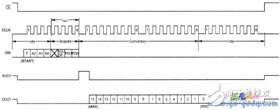
In this paper, the external clock mode works, that is, the ND shift clock is provided by the PIC16F73, and the external clock controls the A/D conversion process and the input clock. When the ADS8341 receives the last bit of the last byte of the control byte, the BUSY pin will be pulled high by the ADS8341. The conversion result will then be asserted and appear on DOUT on the falling edge of the next 16 clock cycles, as shown in the following sequence. The busy state BUSY in the external clock mode is held high until the MSB is asserted. It takes one clock cycle. It takes 16 clock cycles for the 16-bit conversion data to be completely output, so that at least 25 clock cycles are required for one data sampling. . Because the PIC16F73 microcontroller connection uses 8Bit to transfer data, this means that an additional transfer must be added to capture the LSB. This takes 32 clock cycles to handle this requirement, with 32 clock cycles per conversion, the first 8 clock cycles. It is used to send the control word, and the sampling result is output from the ADS8341 in the next 24 clock cycles. The first clock cycle of the last 8 clock cycles is used to capture the LSB bits, leaving the last 7 clock cycles free.

Ejector Header Connector,Dual Row Ejector Header Connector,Single Row Ejector Header Connector,Gold Plated Ejector Header Connector
Shenzhen Jinyicheng Electronci Technology Co.,Ltd. , https://www.jycconnector.com
