With the continuous advancement of storage technology, the storage capacity of Flash Memory is getting larger and larger, and the number of reading and writing is getting faster and faster. The performance price ratio is getting higher and higher. However, NAND Flash itself has shortcomings, which can be summarized in two ways: complex read and write control timing and bit swapping (o, 1 inversion). The NAND Flash device can reuse the instruction, address and data bus, thus saving the number of pins, but the pin not only bears the function of the data bus, but also bears the functions of the address and the instruction bus, so the interface control timing is complicated. The problem of bit reversal is more common in NAND Flash. NAND Flash vendors recommend using NAND Flash while using the EDC/ECC check algorithm.
The NAND Flash controller implemented in this paper is placed between the CPU and the NANF Flash device, and realizes the non-bonded interface of the NAND Flash, which can greatly simplify the operation timing of the CPU to the NAND Flash and improve the use efficiency of the CPU. The ECC function can ensure the accuracy of the stored data. The ECC module and the main control module are relatively independent. When the ECC function is not required, the ECC module is not enabled, which is convenient and flexible.
2 control interface circuit featuresThe entire control circuit 121 is divided into two major functional modules: the first functional module is the main controller module, which simplifies the interface timing of NAND Flash, and can design a Glueless Inter-face for NAND Flash. This makes the timing complexity of NAND Flash operations much less, making the NAND Flash interface map to a non-bonded interface similar to SRAM. The second functional module is the ECC module, which corrects single-bit errors and detects double-bit errors for 512 bytes, but cannot correct for single-bit errors or more. The error of two bits with E is not guaranteed to be detected.
The two functional modules are relatively independent. The ECC function module is located between the main controller module and the NAND Flash chip. It can be selected to work and not work. All commands of the main controller module are transmitted to the NANDFlash chip through the ECC module. When the ECC module is not working. The ECC module is equivalent to connecting the main controller module to the NAND Flash chip; when the ECC module is working. Only some steps will be added to the operation of the controller module, and the operation timing of the main controller module will not be disturbed.
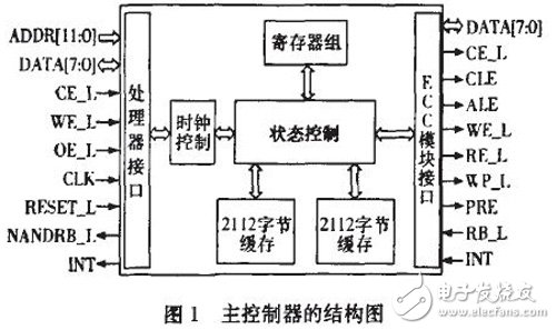
3 main controller 3.1 register and cache configurationThe external interface of the main controller is similar to SRAM, however SRAM has only two main operations, read and write. In addition to r page programming and read operations, NAND Flash also has ID read, reset, block erase and status read operations. It can only use write control words similar to NAND Flash without changing the interface. the way. The main controller has a 16-byte register bank that can read instructions and addresses from the I/O bus. The instruction register is addressed by the Memory Mapped Register. That is, the address of the register is uniformly programmed into the memory space from 0xFF0 to OxFFA.
3.2 Implementation of the main controllerThe block diagram of the main controller is shown in Figure 1. The design implementation of the clock control module and the state control module are discussed separately below.

(1) Clock control module. For this type of read and write enable is an active low chip, the use of a clock with a duty cycle of 1:1 for read and write operations is not cost-effective to increase data access speed. For example, when performing a read operation, RE_L must at least ensure a low level of 35 ns to ensure that the data is correctly read. After RE_L rises to a high level, it is only necessary to ensure that the data is held for another 10 ns, thus adding a margin of 5 ns. The clock cycle must be at least 80ns. To ensure that the data can be read correctly and to maximize the read speed, we use a 16.7MHz clock with a period of 60ns and a duty ratio of 1:2. In this case, the low level duration is 40 ns, and the 35 ns data is sure to be read, there is still a 5 ns margin, and the high level has 20 ns time, which is also abundant, which ensures the correct reading of the data. The performance of the device is fully utilized.
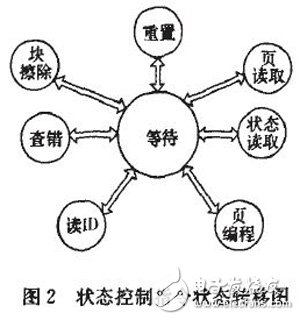
(2) State control module. As shown in Figure 2, the main controller performs controllable
NAND Flash performs reset, block erase, page read, error check, and read ID. The operation of page programming and status read instructions does not support random read and write operations to NAND Flash. When the address input is 0xFFA, the command word in the instruction register is read, the instruction to be executed next is determined, and then transferred to the corresponding state.

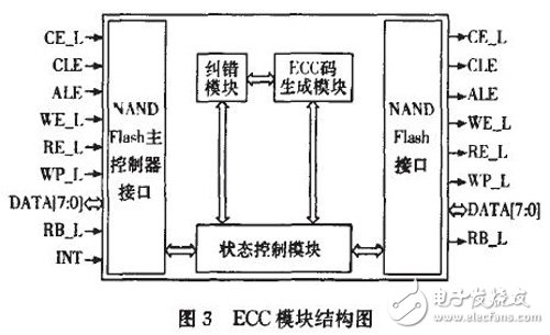
NAND Flash devices are subject to bit swapping, and in some cases one bit will be inverted. This section discusses the design and implementation process of the ECC (Error CorrecTIon Code, ECC for short. The ECC module is placed between the NAND Flash device and the main controller. The ECC module receives various signals from the main controller and does not need to work. When the signal is directly transmitted to the NAND Flash, the control signal of the main controller is intercepted when necessary, and the operation is added to the NAND Flash after adding seven operations. The structure of the ECC module is shown in FIG.

(1) Check code generation module. The ECC check code generation module has a 96-bit (12-byte) arithmetic register for temporarily storing data during operation, and is divided into four groups of three-byte registers, each of which holds a parity value (that is, an exclusive OR of each bit). Value), the value of these registers is updated each time the data is sent. The calculation of these parity flags is based on the sequential position of each byte of data and the data itself.
The shockproof pressure sensor is the most commonly used sensor in industrial practice. It has shockproof function and has a certain benign response in case of various shaking. It is widely used in various industrial automatic control environments, including water conservancy and hydropower, railway transportation, intelligent construction, production automatic control, aerospace, military industry, petrochemical, oil well, electric power, ship, machine tool Pipeline and many other industries.
The integrated sensor is manufactured with standard process technology for producing silicon-based semiconductor integrated circuits. Usually, some circuits used for preliminary processing of the measured signal are also integrated on the same chip.
Shockproof Pressure Sensor,Vibration-Resistant Pressure Sensor,Shock Resistant Pressure Sensor,Waterproof Shockproof Pressure Sensor
Taizhou Jiabo Instrument Technology Co., Ltd. , https://www.jbcbyq.com
