Abstract: ADV7183 is Analog Devices Inc. (ADI) introduced an integrated 10-bit ADC is an enhanced video decoder. It contains two 10-bit accurate analog-to-digital converters (ADCs) and a complete automatic gain control (AGC) circuit, which can be widely used in many systems such as projectors, digital TVs, DVD recorders and game consoles. Paper describes in detail the features of its structure, function and operation principle of the pin, which gives the typical application circuit.
1 Overview
ADV7183 is an integrated video decoder. It can automatically convert an analog video baseband signal compatible with international standards NTSC or PAL into another 16-bit / 8-bit CCIR601 / CCIR656-type YCrCb 4: 2: 2 or 4: 1: 1 video data. Its flexible digital output interface can complete the video decoding and conversion functions in the system based on the buffer structure and line lock clock, which makes the ADV7183 can be widely used in many systems such as projectors, digital TVs, DVD recorders and game consoles. ADV7183 main features are as follows:
â— There is a line lock system clock (LLC) and an adaptive digital line length tracking (ADLLT) circuit inside, which can provide dual video lock function;
â— With three-line chroma comb filter;
â— With real-time clock and information output function;
â— With complete AGC and clamp control functions, programmable video adjustment of chroma, brightness, saturation and contrast;
â— There are 6 analog video input channels;
â— Can be set to two-wire continuous bidirectional port mode, and compatible with I2C?
â— NTSC or PAL detection can be performed automatically;
â— With different modes of video input and 16-bit width bus digital output;
◠The input peak-to-peak value is 0.5V ~ 2V.
figure 1
2 pin function
1 (top view) of the ADV7183 pin arrangement shown in FIG. It uses 80-LQFP package. The definition of each pin is as follows:
(VS / VACTIVE) 1 pin: dual-function multiplexing pin, when (OM_SEL [1: 0] = 0, 0)? This pin outputs a vertical synchronization signal VS corresponding to YUV pixel data; : 0] = 1, 0 or 0,1) when, VACTIVE is a valid signal in the valid period of the video field.
(HS / HAACTIVE) 2 feet: dual function pins (when (OM_SEL [1: 0] = 0, 0), the output is a programmable line synchronization signal HS; and when (OM_SEL [1: 0] = 1 , 0 or 0,1), HACTIVE is a valid signal during the active video line.
(DVSSIO) 3, 14 feet: digital input / output ground.
(DVDDIO) 4,15 feet: digital input / output power supply terminal? 3.3V ?.
(P15 ~ P0) 5 ~ 8, 19 ~ 24, 32, 33, 73 ~ 76 feet: video pixel output port, which includes 8 bit brightness signal Y (P15 ~ P8) and 8 bit color difference signals Cb and Cr (P7 ~ P0) .
(DVSSS1 ~ 3) 9,31,71 feet: digital power ground.
(DVDD1 ~ 3) 10,30,72 feet: digital supply (3.3V).
(AFF) 11 feet: almost full sign. When the FIFO reaches the almost full edge set by the user, this pin is the FIFO control signal indicator.
(CLKIN) 16 feet: asynchronous FIFO clock.
(LCLREF) 25 feet: clock reference output.
(GPO [3: 0]) 17,18,34,35 feet: general purpose output controlled by I2C.
(LLC2) Pin 26: Two-way frequency of the clock output of the line lock system (13.5MHz).
figure 2
(LLC1 / PCLK) Pin 27: dual-function multiplexed pin? Line lock system clock output or FIFO output clock of 20 ~ 35MHz.
(XTAL1) Pin 28: The second pin of the crystal oscillator. If an external clock source is used, this pin may not be connected.
(XTAL) Pin 29: 27MHz crystal oscillator input pin or input connected to an external crystal oscillator (compatible with CMOS level).
(PWRDN) 36 feet: low power enable.
(ELPF) 37 pin: This pin is mainly used for the external loop filter necessary for LLC phase-locked loop.
(PVDD) 38 feet: power supply.
(PVSS) 39 feet: ground.
(AVSS) 40, 47, 53, 56, 63 feet: analog power ground.
(AVSS1 ~ 6) 41, 43, 45, 57, 59, 61 feet: analog input channel. If single terminal mode is selected, then grounding? When a different mode is selected, it is directly connected to REFOUT.
(AVDD) 50 feet: analog power pin (5V).
(CAPY1-2) Pins 48 and 49: ADC capacitor network.
(SDATA) 67 feet: Serial data input / output of MPU port.
(REFOUT) Pin 51: Internal reference voltage output.
(CML) 52 feet: ADC public mode.
(SCLK) 68 feet: MPU port serial clock input interface.
(CAPPC1 ~ 2) Pins 54 and 55: ADC capacitor network.
(ALSB) Pin 66: TTL address input.
(ISO) Pin 65: The input exceeds the switch. 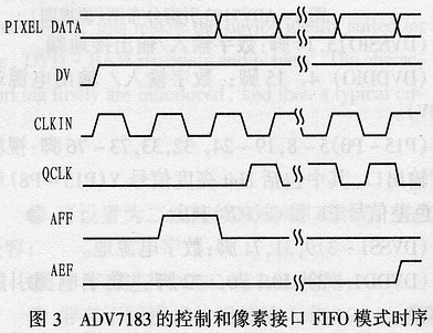
(AIN1 ~ 6) 42,44,46,58,60,62 foot: analog video input channels.
(VREF / VRESET) 69 feet: VREF marks the beginning of the next game; VRESET marks the beginning of a new field.
(HREF / HRESET) 70 feet: HREF marks the start of a new video line; HRESET marks the start of a new line.
(RD) 77 feet: asynchronous FIFO read enable signal.
(REST) ​​Pin 64: The system input is reset.
(DV) Pin 78: Data valid output signal.
(OE) Pin 79: Output enable control port.
(FIELD) Pin 80: Odd / even field output signal.
3 works
The internal principle and functional block diagram of ADV7183 are shown in Figure 2. The working principle is introduced below.
3.1 Analog signal input
The ADV7183 has 6 analog video input channels. These 6 channels can support 6 CVBS input signals, 3 S-vido input signals, and 2 YCrCb analog video input signals with different configurations. The type of input and channel selection can be controlled through INSEL. The analog signal input front-end includes three clamping circuits for DC recovery. There are three sample-and-hold amplifiers before the ADC, which can ensure that the sampled values ​​reach three channels at the same time in the YCrCb input mode. Two 10-bit ADCs are used for sampling. In order to capture video signals with the highest possible quality, there is a big difference in the entire analog signal input front end.
3.2 Synchronous pixel output interface
ADV7183 supports three output interface modes: synchronous pixel interface compatible with LLC, CAPI interface and SCAPI interface. When set to synchronous pixel interface mode, the output of pixels and control data is synchronized with LLC1 (8-bit mode) or LLC2 (16-bit mode). In this mode, the field blanking, row blanking, and column blanking control and timing information coding is the same as the control code. When set SCAPI CAPI interface or interface mode, only the active output only pixel data of synchronous and asynchronous FIFO clock (CLKI). Pixels are generally output through a 512-pixel deep, 20-bit wide FIFO container. The HACTIVE and VACTIVE outputs generally use independent pins. The interface mode data of the CAPI interface and SCAPI is always 16-bit, so when the output interface requires 8-bit or 10-bit, this interface mode cannot generally be used. ADV7183 default mode of the LLC compatible 8-bit CCIR656 4: 2: 2.
Figure 4
3.3 Control and pixel interface FIFO mode
Figure 3 shows the timing of the ADV7183 control and pixel FIFO interface mode. When the ADV7183 works in this mode, the generated pixel data will be cached in the 512-pixel deep FIFO container. Only the active video pixels and control codes are written to FIFO, and the rest are discarded. In this mode, CLKIN must be faster than the effective data rate moved into FIFO, otherwise FIFO will overflow. When operating in SCAPI ADV7183 interface mode may be utilized DV (data valid) to the RD (read enable) of the feedback system to ensure that no FIFO overflow. And when FIFO reaches AFF (almost fuzzy), the DV immediately rises and keeps the FIFO as AEF (almost empty). When using this mode, the output pixel data DV and QCLK indicators may be determined.
4 Typical applications
Figure 4 is a typical application circuit of ADV7183. Among them, the power supply voltage of the circuit should be selected as 7V, VDD should be selected as 4V, the digital input pin voltage should be GND-0.5V to VAA + 0.5V, and the analog output voltage should be GND-0.5V to VAA. The circuit can work in the temperature range of 0 ~ 70 ℃. Also need to pay attention: ADV7183 is ESD (Electronic Status) sensitive equipment. Although ADV7183 itself with ESD protection circuit, but the damage sustained by the high-intensity electrostatic discharge, ADV7183 can cause performance degradation and functional decline, so? It is necessary to take appropriate ESD protective measures.

Follow WeChat

Download Audiophile APP

Follow the audiophile class
related suggestion
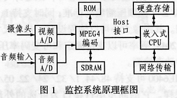
Abstract: IME6400 Korea INTiME developed to support high-resolution real-time video encoding MPEG4 integrated circuit ...
Three-terminal ...
![[Photo] Three-terminal voltage regulator XWY2005 and its application](http://i.bosscdn.com/blog/20/06/41/7212011242.jpg)
...
High Accuracy CMOS Operational A ...
![[Photo] High-precision CMOS operational amplifier LMC6062 / ...](http://i.bosscdn.com/blog/20/06/41/6175842568.gif)
Abstract: NCP1
![[Photo] Single-ended PWM controller NCP1205 and its application](http://i.bosscdn.com/blog/20/06/41/6173136914.gif)
NE605 is Philips ...
![[Photo] High performance small power FM receiver chip NE605 and its application ...](http://i.bosscdn.com/blog/20/06/41/5192033610.gif)
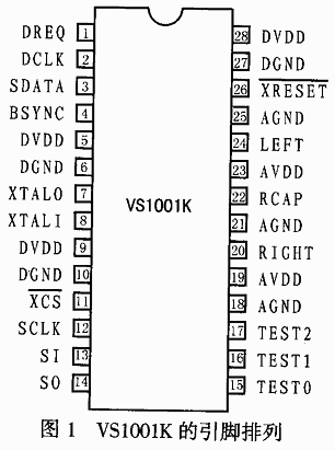
Abstract: VS1001K is a new MP3 decoder chip produced by VLSI Solution of Finland. The chip contains high quality ...
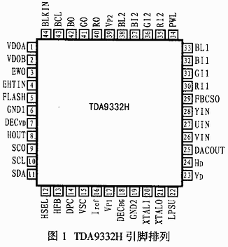
Abstract: TDA9332H is a display processor suitable for high-end color TV produced by Philips, which can be used for single scan (50 or 60Hz) and dual ...
Introduction
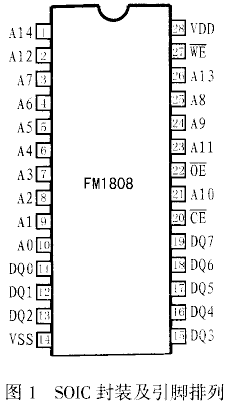
Summary: High Performance Parallel Interface ferroelectric memory RAMTRON produced FM1808 NV-SRAM is ideal alternative ...
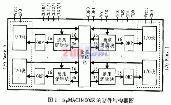
Abstract: The features of Lattice Semiconductor has introduced ultra-fast zero-power complex programmable logic devices in the ispMACH4000Z, ...
This article introduces the main features, pin functions, software design, hardware connection and specific application circuit of PTR2030. PTR2030 is super ...
XTR110 American Burr - Brown has introduced a precision voltage / current converter, which is designed for analog signal transmission ...
Abstract: This article introduces the MAX712 / MAX713 programmable battery charge management chip produced by MAXIM, using MAX ...
Abstract: This article introduces the principle, characteristics and pin functions of the embedded microprocessor MCF5249 of MOTOROLA company, and explains ...
Abstract: Based on the analysis of the ARM architecture, the structural characteristics and advantages of the 32-bit ARM core processor W90N740 are introduced ...
Abstract: This article introduces in detail the basic principles, features and original use of the digital tube and keyboard smart chip zlg7289A ...
Abstract: This article introduces the structure, function and interface characteristics of OMAP5910, and ...

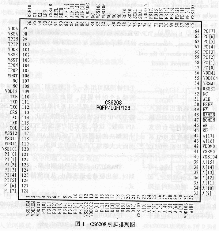
Abstract: CS6208 is Myson Century introduced a chip specifically for network control and transmission, which is based on 80 ...
