
First, the basic requirements and principles input voltage AC (90 ~ 265V), frequency (47 ~ 440Hz); output DC voltage 12V / 24W, efficiency η = 70%, linear adjustment <1% × output voltage, ripple and noise ≤ 2 % × output voltage (mVP-P), with over-current, over-voltage, short-circuit automatic recovery and other protection functions. The basic principle is shown below.
When VT is turned on, the current in the primary winding N1 of the transformer increases linearly, the magnetic field is enhanced, and the internally generated induced electromotive force is generated in the direction of the upper and lower negative, and is coupled to the secondary coil N2 through the magnetic core. According to the principle of the same name, the induced voltage direction is upside down and positive. At this time, the diode VD connected to N2 is in a reverse bias state, VD is turned off, and no current flows in N2, that is, no energy is transmitted to the load RL.
When VT is turned off, the current in the transformer primary winding N1 will disappear. Since the current cannot be abruptly changed, the electromotive force & epSILon is induced in Nl; the direction of change is positive and negative. Try to maintain the original state. The magnetic field in N1 is coupled to the secondary coil N2 through the magnetic core. According to the principle of the same name, the induced voltage direction is up and down, and the diode VD connected to N2 is in a positive bias state, and VD is turned on to charge the output capacitor C. At the same time, the current IL flows through the load RL.
The so-called back-excitation means: VT conduction → primary Nl energy storage → VD cut-off → no current in secondary N2; VT cut-off → primary N1 discharge → VD conduction → secondary N2 has current. The so-called single-ended is relative to bridge or push-pull.

Second, the circuit schematic diagram and the working process analysis circuit schematic diagram shown below. 220V AC-Power Noise Filter (PNF) filters out RF interference-rectifier (VD5~VD8) and Cl filter to obtain about +300V DC voltage. The voltage is divided into two ways: one through the Nl winding → D1 of VT1, the other is stepped down by R15 and provides a starting voltage of about +13V to IC1. IC1 internal oscillation, IC16 pin output switch pulse → VT1 is in the switch state → Nl The winding produces a varying magnetic field: on the one hand, it is coupled to the feedback winding N3 → rectification filter (VD2, C3) → the output +13V voltage supplies power to IC1. On the other hand, it is coupled to the secondary winding N2 → rectification (VD4) → filtering (Cll-C14, 12) → output +12V voltage. C2, VD1, Rl and R12 form an absorption loop for absorbing peak voltage and protecting the switching tube. R5, R6, VD3 and R7 form a gate passive acceleration shutdown driving circuit. When the IC16 pin is from "1" to "0", it can accelerate the rapid bleed of the G-pole charge of the MOSFET to reduce the turn-off loss.
In order to stabilize the output DC voltage, a voltage regulator circuit is provided in the circuit. If the voltage of the VD4 rectified output terminal is higher than the rated value, the voltage at the R terminal of the precision sampling circuit IC2 of the resistor RH1 and VR is also increased accordingly → the voltage of the K terminal of IC2 is lowered - so that the voltages flowing through the IC2 of the photocoupler IC2 The current is increased, the brightness of the internal light-emitting tube is increased, so that the resistance between the 3 and 4 pins of IC2 is decreased. → The potential of the 1 pin of IC1 is decreased. After the internal circuit of IC2 is processed, the square wave pulse of the 6 output is narrowed → the switching tube VT1 is The on-time is shortened - the energy transmitted by the switching transformer T1 is reduced → the induced voltage of the secondary winding N2 is decreased → the output voltage is decreased → thereby achieving the purpose of the regulated output. Adjusting the size of the VR allows the output to be adjusted within ±10%.
In order to protect the power supply itself from the load, a protection circuit is provided in the circuit. When the external current causes the current flowing through the switching tube VT1 (2N60C) to increase → the current flowing through the sampling resistor R2 also increases accordingly → the voltage of the IC 13 rises after R3. When the voltage of the foot is greater than 1V→N301 internal oscillation circuit automatically stops vibrating→to achieve the purpose of overcurrent protection. When the output is over-voltage → Zener diode Z1 breakdown → PC2 (photocoupler) 1, 2 feet → internal LED light-emitting → PC2 4, 6-foot thyristor conduction → vCC voltage drops to OV → IC1 stops oscillation → The output is reduced to Ov→ to protect the output load.
In addition, when the external factor causes the IC17 pin voltage to be lower than 10V or higher than 34V, the overvoltage and undervoltage detection circuit inside the IC can automatically cut off the IC16 pin output square wave pulse, then the switching power supply is stopped, thus reaching overvoltage and undervoltage. The purpose of protection.
Third, the choice and role of components
1. The input circuit power supply noise filter L1 (PNF) mainly prevents the high frequency interference of the power supply from entering the power grid, and also prevents the interference in the commercial power from entering the power supply.
The current limiting resistor TH1 generally selects a PTC component with a resistance value of about 10 Ω, and the impedance is usually low, and there is no heat. The voltage is mainly dropped on the system. When the fault current of the system is abnormal, TH1 voltage drop increases and heats up. The PTC component is a positive temperature coefficient component. The higher the temperature, the higher the resistance (up to 100 K). The 220V is almost fully added to TH1, and the system is protected by power loss.
After power failure to remove the fault, after a period of heat dissipation, TH1 returns to normal resistance. Can work normally. TH1 also limits the inrush current during startup.
Varistor ZNR, rated voltage can be 470V. When an overvoltage occurs, the ZNR undergoes non-invasive breakdown. Due to the TH1 heating protection, TH1 and ZNR can be recovered as long as the overvoltage is removed and the power is turned off for a period of time.
Rectifier. The average value of the rectified output voltage (UO) is equal to 1.2-1.3 times the effective value (UIN) of the input voltage. According to Po=UocimxIO×η=24W, the minimum rectified output voltage UDCmin≈90V, the efficiency η is set to 80%, and the rectified output current is Iåº0.33A. Select the rated current and rated voltage of the rectifier to have a margin of 3 times. The IN4007 meets the requirements.
The filter circuit plays a very important role in limiting the ripple size in the rectified output voltage. In the full voltage input range, the maximum output voltage of the rectifying and filtering circuit can reach 370V, so the withstand voltage of the filter capacitor should be ≥400V. The capacity selection principle is ≥1μF/W, and this example selects 47μF/630V.
2. The switching circuit has three parts: the peak voltage, the reset voltage and the power supply voltage in the voltage waveform of the main switching tube. Under the AC220V voltage application condition, if the power supply voltage variation range is ±20%, it is in the single-ended flyback type. The withstand voltage of the switch tube should be 600~700V. Set the maximum duty ratio to 0.4 (corresponding recoil voltage UR is 133V), the efficiency T1 is 80%, the circuit works in the current interrupt mode, and the output current of 1A can output 30~32W output on the switch tube. power. Considering the effect of the on-resistance of the switching tube on the efficiency, the rated current of the switching tube should be selected to reach 3 to 4 times the peak value of the actual flowing current. In this case, 2N60C is selected, and the parameter is 12A600V. VD1 and VD3 use recovery diode FR305.
3. Pulse width modulation (PWM) circuit
The UC3842 is a high-performance fixed-frequency, current-mode PWM controller from Unitrode that includes an error amplifier, PWM comparator, PWM latch, oscillator, internal reference supply, and undervoltage lockout. The UC3842 voltage regulation rate can reach 0.01%, the operating frequency is 500kHz, the starting current is less than 1mA, the reference voltage is 4.9~5.1V, the operating temperature is O°C~70°C, and the output current is 1A. The input voltage is 10~34V. When it is lower than 1OV, the circuit stops and the external MOSFET power tube is turned off. The frequency of the output switching pulse is affected by the peripheral timing components (R4, C4) of the 4 pin, and the duty ratio of the output is changed by the parameters of the 1st and 3rd feet, thereby achieving the purpose of adjusting the output voltage.
4. When the output rectification filter circuit outputs a low voltage (such as 5, 3.3V or lower), the Schottky diode is often used as a rectifier because it has a forward voltage reduction characteristic to obtain a relatively low loss. When the output is around 12V, both ultra-fast recovery diodes and Schottky diodes are available.
Since the ripple current of the flyback switching power supply output is large, the output filter capacitor is calculated by 1000μF for each output 1A current, and a brand with lower equivalent series resistance such as KORChip should be used. In this case, 1000 μF is selected.
5. The output regulation reference output regulation reference is TLA31.
6. The output protection circuit output overvoltage protection circuit is composed of a photocoupler (MOC3022) and a Zener diode 21 (15V, 0.5W) driven by the thyristor. The minimum blocking voltage peak of PC2 (MOC3022) is 400V, the LED trigger current IFT (VTM=3V) is lOmA, and the output drive current is 1A.
Fourth, the design and winding of the transformer
1. The power of the transformer core selection flyback converter is relatively small. Generally, the core of the ferrite material is selected, and the power capacity (AP) is calculated as: AP=Ae×AQ. According to the calculated AP value, a magnetic core with a larger margin can be selected. In this example, the EFD25 ferrite core is selected, and its effective cross-sectional area is larger than the calculated value.
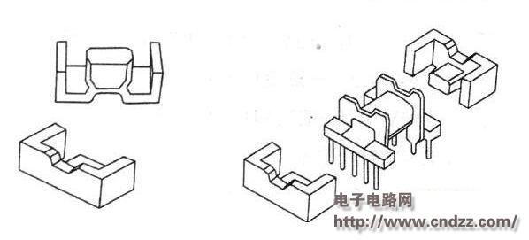
The shape of the EFD25 core is shown below.
2. The number of turns and the wire diameter are calculated in the AC 90-265V voltage input range. In order to improve the efficiency of the switching transformer, the AC220V voltage level should be in the current interrupted state, while the AC110V is the current continuous state.
When the current is interrupted, since the lower limit value of AC220V voltage level is AC176V, the rectified and filtered DC voltage can be based on 200V as the basic parameters. The calculation parameters for the primary winding are: current peak value Ip, current effective value IPrms, inductance LP, number of turns N1p, air gap lg, wire diameter φp (current density is 3A/mm 2 ); calculation parameters for the secondary winding are: current peak ISm, current effective value 1Srms, number of turns Ns, wire diameter φs ( The current density is 3A/mm 2 or slightly higher).
When the current is continuous, since the lower limit of the AC110V voltage level is 85V, the rectified and filtered DC voltage can be based on 90V as the basic parameters. The parameters to be calculated are: duty cycle DMAx, primary winding current peak iP. As long as the iP to IP ratio is about 107%. In addition, the number of turns of the sampling winding can be derived from N1p, Ne according to the sampling output voltage (13V).
The coil diameter and the number of turns in this example are shown in the following table. The skeleton and combined structure are shown in the left and lower right figures. 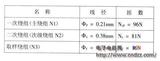
3. The winding method should aim at reducing the leakage inductance of the transformer in the winding of the switching transformer. A common method is to divide the primary winding into two segments, which are wound around the inner side and the outer side of the secondary winding, respectively. That is, the innermost layer of the secondary winding is the first layer of the primary winding, and the outermost layer is the third layer of the primary winding. In this way, there should be extra pins on the skeleton to connect the center points of the primary windings.
The first layer and the third layer may be wound in a manner of 1/2 or a small number of layers of the first layer, and the second layer is wound by four wires, and the fourth layer is a sampling winding layer. The winding transformer T1 winding direction and the steps are as follows:
Fifth, the design of the PCB
The main components on the PCB are distributed on the left and right sides, while the right side is divided into upper and lower parts. The left side is mainly composed of a filter capacitor C1, a switch circuit composed of a primary winding N1 of the switch tubes VT1, T1, and a control circuit composed of a UC3842; the upper part of the right side is a power supply noise filter circuit, and the lower part is a power supply rectification output, a voltage regulator, and Protection and other circuit components.
In terms of structure, a metal case with good heat dissipation is selected, and in this case, an aluminum case is selected. The filter capacitor C1 needs to be installed horizontally, and the switch transformer T1 adopts the EFD25 type skeleton, which belongs to the horizontal installation. In this way, the device height is limited. A component that generates a relatively large power consumption, such as a switching transistor VT1 and an output rectifier VD4, is provided with a heat sink.
In the layout of the printed strip, it is necessary to solve the problem of EMI (electromagnetic interference). The solution is to strictly separate the switch and oscillation control circuit part from the rectified output part, and use optical coupling isolation in the middle to prevent the oscillation interference signal string from being output. The printed strips on the upper and lower sides of the PCB are also separated, and the PCB is also cut to prevent the upper power supply noise filter (PNF) from interfering with the lower rectified output. In addition, SMT components should be used in the oscillation part of the switch, and a large-area printed strip process should be adopted at the output end.
Industrial PC, a Fan-less cooling and smallest case allows for space-saving design, so it can be placed horizontally or vertically to offer you best placement options, and you`ll set it on a desk and forget its even there.
Low cost mini pc, Personal computer, Miniconputer, Industrial PC, Mini pc windows
Shenzhen Innovative Cloud Computer Co., Ltd. , https://www.xcypc.com