
Double-click [Xilinx Core Generator] to open an existing IP core project or create a new IP core project. [View by funcTIon] → [Debug & VerificaTIon] → [ChipScope Pro], double-click VIO. The VIO configuration page is displayed, as shown in Figure 9-10.
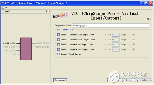
Figure 9-10 VIO parameter setting interface
(1) [Component Name]: Enter the component name.
(2) VIO Parameters option group: VIO parameter option group.
[Enable Asynchronous Input Port]: Enable asynchronous input signal, up to 256 asynchronous input signals. The asynchronous input of VIO is used to monitor the output signal of the module to be tested in the design. It is independent of the clock.
[Enable Asynchronous Output Port]: Enable asynchronous output signal. Up to 256 asynchronous output signals can be set. The asynchronous output of VIO is used to provide input excitation for the logic module to be tested. It is independent of the clock.
[Enable Synchronous Input Port]: Enable synchronous input signal, up to 256 synchronous input signals. The synchronous input signal of VIO is used to monitor the output signal of the module to be tested in the design, and the signal to be tested is synchronized with the CLK of the VIO core. .
[Enable Synchronous Output Port]: Enable synchronous output signal. Up to 256 synchronous output signals can be set. The synchronous output signal of VIO provides excitation for the input of the module to be tested, and the signal to be tested is synchronized with the CLK of the VIO core.
[Invert Clock Input]: The VIO core can select the clock signal to be flipped, that is, the rising or falling edge of the clock is selected as the trigger condition.
Note: Clock signal flipping is only effective when using synchronous inputs and/or outputs.
9.2.4 ATC2 Attributes
Double-click [Xilinx Core Generator] to open an existing IP core project or create a new IP core project. [View by funcTIon] → [Debug & VerificaTIon] → [ChipScope Pro]. Double-click ATC2 to bring up the ATC2 configuration interface, as shown in Figure 9-11.
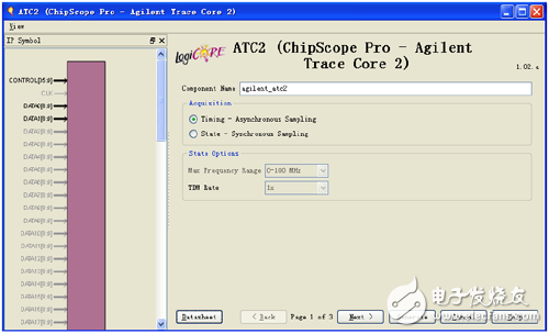
Figure 9-11 ATC2 parameter setting interface
(1) [Component Name]: Enter the component name.
(2) Acquisition option group:
[Timing – Asynchronous Sampling]: Used for asynchronous data capture. The channel through which the data signal is output to the FPGA pin via the ATC core consists of combinatorial logic.
[State - Synchronous Sampling]: Data capture for synchronization with the CLK input signal. The channel through which the data signal is output to the FPGA pin via the ATC core consists of a pipeline flip-flop and a CLK input signal.
(3) State Options: Status option group.
[Max Frequency Range]: The maximum frequency range of the ATC2 core. The valid maximum frequency options are 0 to 100 MHz, 101 to 200 MHz, 201 to 300 MHz, and 301 to 500 MHz. When the target data capture mode is set to [State - Synchronous Sampling], this selection is valid for the ATC2 core.
[TDM Rate]: The ATC2 core does not use on-chip memory to store captured data. The Agilent logic analyzer transmits the captured data through a dedicated probe connector and FPGA pin connection. The ATC2 core data can be transferred to the FPGA pin at the same rate as the ATC2 input port DATA (TDM rate = 1x) or twice the DATA rate (TDM rate = 2x). Only when the target data capture mode is set to [State - Synchronous Sampling], the TDM rate can be set to 2 times the data rate.
After setting, click [Next] to pop up the pin setting interface, as shown in Figure 9-12.
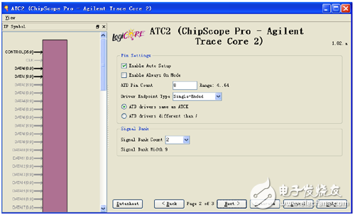
Figure 9-12 ATC2 core ATCK and ATD pin parameters
(4) Pin Settings option group: Pin setting option group.
[Enable Auto Setup]: Enables the Agilent logic analyzer to automatically set the connection between the ATC2 core pin and the logic analyzer POD. This property allows the Agilent logic analyzer to automatically set the optimum phase and voltage sample offset for each ATC2 pin. The default is enabled.
[Enable Always On Mode]: Used to force the ATC2 core to enable the ATC2 core internal logic and output buffer. This mode forces BANK0 to be selected after the FPGA configuration is completed. In this mode, the device can be captured immediately after the configuration is completed without manually setting the ATC2 core. This option is valid only when the target data capture mode is set to [TIMING] mode.
[ATD Pin Count]: Set the number of ATD output pins, ranging from 4 to 128.
[Driver Endpoint Type]: Used to set the output driver type for controlling the ATCK and ATD output pins: single-ended or differential. All ATCK and ATD pins must be set to the same drive terminal type.
[ATD drivers same as ATCK]: ATCK pin parameters such as I/O standard, SLEW parameters and drive strength can be modified, and the ATD driver parameters are forced to be consistent with the ATCK driver parameters.
[ATD drivers different than ATCK]: The driver parameters of each pin of ATD can be set separately, completely independent of ATCK.
(5) Signal Bank option group: Signal Bank setting option group.
[Signal Bank Count]: The ATC2 core contains a real-time selectable data signal group multiplexer. This option represents the multiplexer input, ie the number of data input ports or the number of signal packets. Valid signal grouping values ​​are 1, 2, 4, 8, 16, 32, and 64.
Tinned Copper Wire,Tinned Copper,Tin Coated Copper Wire,Tin Plated Copper Wire
Sowell Electric CO., LTD. , https://www.sowellsolar.com