1 Introduction
With the continuous improvement of application requirements, many embedded systems require expanded large-capacity memory to store data in their applications. CF card (CompactFlsahCard) is widely used in embedded products due to its low price, large storage capacity, small size, and good compatibility. However, the existing CF card interface circuit has disadvantages such as complicated interface and low stability, which cannot meet the needs of customers. Through in-depth study of the external bus interface (EBI) of the ARM processor AT91RM9200, the working principle of CF card and CPLD, it is proposed to use CPLD to improve the CF card interface circuit to solve the shortcomings in the existing interface circuit.
2 device introduction
2.1 External bus interface
The system uses AT91RM9200 with ARM920T as the core as the microprocessor. It is a system built entirely around the ARM920Thumb processor. It has a wealth of system and application peripherals and standard interfaces, including a high-speed on-chip SRAM work area and a low-latency external bus interface (EBI) to complete the off-chip storage area and internal memory mapping peripheral configuration required by the application Seamless connection. The external bus interface structure is shown in Figure 1.
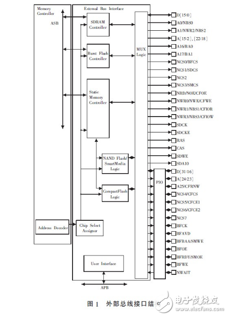
EBI supports the CF card and SmartMedia protocol through integrated circuits, which greatly reduces the need for external components. In addition, EBI can handle the data transfer of up to 8 peripherals, and each peripheral is allocated 8 address spaces defined in the built-in memory controller. Data is transmitted through a 16-bit or 32-bit data bus, the address bus is up to 26 bits, 8 chip select ports (NCS [7:0]) and multiple control pins multiplexed between different external memory controllers are multiplexed .
2.2 CF card
CF card (CompactFlashCard) is a memory card using FlashMemory technology, which has the advantages of small size, low price, strong compatibility, and large storage capacity. The CF card supports three interface modes, namely PCCardMemoryMode, PCCardI/OMode, and TrueIDEMode. Because TrueIDEMode is not often used, the interface circuit is designed with PCCardMemoryMode and PCCardI/OMode.
2.3CPLD
CPLD (ComplexProgrammableLogicDevice) is a logic element that is more complex than PLD [2], and is a digital integrated circuit in which users construct logic functions according to their own needs. The basic design method is to use the integrated development software platform, use schematic diagrams, hardware description language and other methods to generate the corresponding target file, and transfer the code to the target chip through the download cable ("in-system" programming) to realize the designed digital system .
The CPLD used in this article is EPM7128SQL100-10 of Altera's MAX7000S series. It has 84 pins, 5 of which are used for ISP (INSystemProgrammable) download, which can be easily programmed "in-system". EPM7128SQL100-10 supports voltage work, and can use Altera's fourth-generation development platform quartus II to easily perform simulation, synthesis and download.
3 hardware interface circuit design
The circuit diagram of the hardware interface circuit is shown as in Fig. 2. In this circuit, CPLD is used to realize the logic functions of some logic devices such as bidirectional buffers and NAND gates in the general CF card interface circuit, so that the interface circuit becomes simpler, stable, and high-speed, and it can be modified by program modification on site. Realize different functions.
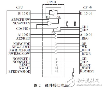
_CD1 and _CD2 in the CF card are the status detection signals of whether the CF card is installed, and they are grounded in the CF card. When the CF card is not installed, the output of _CD1 and _CD2 are pulled to high level by the pull-up resistor in the circuit; when the CF card is installed, _CD1 and _CD2 are output to low level by the ground of the CF card, and _CD1 and _CD2 are equivalent to The main switch of the CF card. In the actual interface circuit, _CD1 and _CD2 should be connected to 10kΩ pull-up resistors.
In I/O mode, the logic of CompactFlash drives the read and write signals of the SMC on the CFIOR and CFIOW signals. At this time, the CFOE and CFWE signals are invalid. In the same general storage mode and flag storage mode, the SMC on the CFOE and CFWE signals is driven, and the CFIOR and CFIOW signals are invalid. The logic is shown in Figure 3.
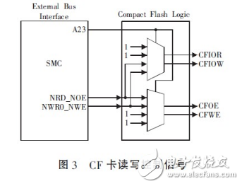
CFOE and CFWE are connected through CPLD and OE of CF card and WE, which is the read and write enable of CF card in MemoryMode.
CFIOE and CFIOW are enabled through I/OMode. Except for the enable signal, the other signals are the same for the two modes.
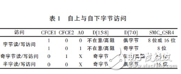
The CFCE1 and CFCE2 signals enable the data bus of the CF card to be accessed from top or bottom. See Table 1 for specific information. Odd byte access can only be performed when the SMC on the NCS4 pin is configured to drive an 8-bit memory. The chip select register in the NCS4 address space must be set as shown in Table 1.
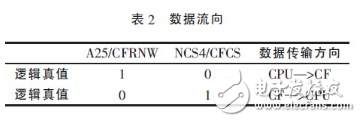
When _CD1 and _CD2 are low, the lower 11 bits A [10:0] of the CPU address bus are connected to the address bus A [10:0] of the CF card, and the lower 16 bits D [15:0] of the CPU data bus Connect with the address bus D [15:0] of the CF card. The A25/CFRNW signal of the CPU is the direction of the data flow, and the NCS4/CFCS signal is the transmission enable of the data bus. Please refer to Table 2 for details.
The CPU is a high-speed device, and the CF card is a low-speed device. When the CPU transfers data to the CF card, data loss occurs due to the slow receiving speed. So it is necessary to delay the sending of the CPU with the _WAIT signal, so that the sending timing of the CPU can be matched with the receiving timing of the CF card, so that the data transmission is correct. In the actual circuit, the _WAIT signal of the CF card controls the NWAIT signal of the CPU through the CPLD, and _WAIT should be connected to a 10kΩ pull-up resistor. RDY/BSY is the working status signal of the CF card. When RDY/BSY is 1, the CF card is ready to receive new data; when RDY/BSY is 0, the CF card is receiving data, this signal should also be connected 10kΩ pull-up resistor. The reset RESET signal of the CF card is also generated after the system reset nRESET signal is inverted in the CPLD to keep it synchronized with the system reset signal.
4CPLD program development
The CPLD program is written in VerilogHDL language under quartusâ…¡. After the program is compiled, it is downloaded to the CPLD for curing. Connect the circuit board and the CF card to read and write data to the CF card. The test results show that the data transmission is correct and the transmission rate is higher.
5 concluding remarks
This article focuses on how to use CPLD to connect ARM-based embedded systems and CF cards. The CPLD used therein not only simplifies the interface circuit and makes it suitable for on-site programming, while the improved interface circuit is also suitable for generating various complex combinational logic and sequential logic. The correctness of this storage technology has been verified on the circuit board, and it provides an effective solution for the CF card storage of ARM-based embedded systems.
Plate-Wire,Tinned Copper Plate Wire,Customizable Color Plate Wire,Black Bamboo Thread
Dongguan ZhiChuangXing Electronics Co., LTD , https://www.zcxelectronics.com
