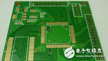
1. Carefully check the schematic: The design of any printed board is inseparable from the schematic. The accuracy of the schematic is the premise of the correctness of the printed board. Therefore, before the design of the printed board, the signal integrity of the schematic must be carefully and repeatedly checked to ensure the correct connection between the devices.
2. Device selection: The selection of components is a very important part of the design of printed boards. Devices with the same function and parameters may have different packaging methods. The package is different, and the solder holes (disks) of the devices on the printed board are different. Therefore, before proceeding with the design of the printed board, it is necessary to determine the package form of each component.
Multilayer boards must be positioned in the selection of surface mount components (SMD) for device selection. SMD is widely used in various electronic products due to its advantages of miniaturization, high integration, high reliability, and installation automation. . At the same time, in the device selection, not only should pay attention to the characteristics of the device should meet the requirements of the circuit, but also pay attention to the supply of the device to avoid the problem of device shutdown; at the same time, it should be realized that many domestic devices, such as chip resistors, capacitors, and connections. The quality of the device, potentiometer, etc. has gradually reached the level of imported devices, and has the advantages of sufficient supply, short delivery time and low price. Therefore, under the conditions of circuit approval, domestic devices should be considered as much as possible.
There are four types of lasers currently used to make microvias for printed circuit boards: CO2 lasers, YAG lasers, excimer lasers, and copper vapor lasers. CO2 lasers are typically used to produce holes of about 75 [mu]m, but because the beam is reflected back from the copper surface, it is only suitable for removing the dielectric. CO2 lasers are very messy, inexpensive, and require no maintenance. Excimer lasers are the best choice for producing high quality, small diameter pores with a typical pore size of less than 10 μm. These types are ideal for high-density array drilling of poly-colloidal substrates in micro ball grid array (microBGA) devices. The development of copper vapor lasers is still in its infancy, but it still has the upper hand when high yields are required. Copper vapor lasers remove both dielectric and copper, but they pose serious problems in the production process, allowing airflow to produce products only in confined environments.
The most common laser used in the printed circuit board industry is a Q-switched QAd:YAG laser with a wavelength of 355 nm in the ultraviolet range. This wavelength allows most metals (Gu, Ni, Au, Ag) to melt when the printed circuit board is drilled, and its absorption rate exceeds 50% (Meier and Schmidt, 2002), and the organic material can also be melted. The photon energy of the ultraviolet laser can be as high as 3.5-7.5 eV, which can break the chemical bond during the melting process. The department passes the photochemical action of the ultraviolet laser, and the department passes the photothermal effect. These machines make UV lasers the first choice for printed circuit board applications.
The YAG laser system has a laser source that provides an energy density (flow rate) of more than 4 J/cm2, which is necessary to drill through the microvia surface. The melting process of organic materials requires an energy density of only about 100 mJ/cm2, such as epoxy resin and polythene. In order to operate accurately over such a wide spectral range, very precise and precise control of the laser energy is required. The micro-via hole drilling process requires two steps. The first step is to open the copper foil with a high energy density laser, and the second step is to remove the dielectric with a low energy density laser.

When the laser has a wavelength of 355 nm, its typical spot diameter is about 20 μm. When the pulse time is less than 140 ns, the frequency of the laser is between 10 and 50 kHz, and the material at this time does not generate heat.
Positioning the laser beam through a computer controlled scanner/reflection system, focusing through the focal lens, allows the beam to be drilled at an accurate angle. The scanning process generates a vector pattern through software to compensate for material and design deviations. The scanning area is 55x55mm. This system is compatible with CAM software and supports all common data formats.
The laser system was proposed by the German MisLPKF. The mechanical design of the base is hard granite with a surface finish of not less than 3 μm. The table support is placed on the gas bearing and is controlled by a linear engine. The correctness of the positioning is controlled by a glass ruler with a repeatability of ±1 μm. The table itself is equipped with an optical sensor that precisely adjusts the laser position at different reflection points to compensate for variations in optical distortion and long-term drift. After adjustment, a series of correction data generated by the software can cover the entire scanning area. Drift scale compensation takes approximately 1 minute to operate. Any change in the substrate, such as the positional deviation reference, can be detected by a high resolution CCD camera and compensated by software control.
This system is very suitable for the production of prototypes, which can be drilled and configured, from flexible to rigid printed circuit boards.
Recommended reading:
Printed circuit board quality requirements _ printed circuit board principle
Printed Circuit Board Basics Summary_Printed Circuit Board Manufacturing Process
Simple DIY printed circuit board design and production process
Aluminum Alloy Notebook Stand,Adjustable Aluminium Alloy Notebook Stand,Aluminum Alloy Notebook Stand Universal,Aluminum Laptop Computer Stand
Shenzhen ChengRong Technology Co.,Ltd. , https://www.dglaptopstandsupplier.com
