
The traditional power data acquisition system is limited by limited storage space and communication interface. It has shortcomings such as low precision, poor real-time performance and small amount of information collected. It can not meet the actual power system scheduling and management needs. The STM32-based based on this paper The new power data collector takes full advantage of STM32's rich on-chip resources, which greatly saves hardware investment. It utilizes STM32's high-performance ADC with fast sampling, advanced power and clock management, and dual watchdog functions, which greatly enhances the system's Real-time and reliability, accuracy is significantly improved, while power consumption is greatly reduced.
1, the overall designThe system consists of analog quantity and switch quantity acquisition module, communication module and host computer human-computer interaction module. The system block diagram is shown in Figure 1. First, the analog signal such as voltage and current is conditioned by the signal conditioning circuit, converted into a digital signal by an analog-to-digital converter ADC, and then processed by STM32; the digital signal is input through the I/O port, and the STM32 is interrupted or queried. Read. After the power data is collected and processed, it is displayed by the LCD screen and stored at the same time to query the historical data. In order to make the data display more intuitive and remote monitoring, communicate with the host computer through RS485.
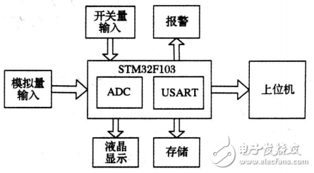
Figure 1 System principle
2, system hardware design 2.1, STM32 on-chip resourcesThe STM32F103ZE12-bit ADC is a successive approximation analog-to-digital converter. Each channel conversion can be performed in single, continuous, sweep or discontinuous mode. The conversion result is stored in a 16-bit data register in left or right alignment. The channel sampling time is programmable, and the total conversion time can be reduced to 1μs. In addition, multiple conversion modes are available to support DMA data transmission. The system uses a timer-triggered synchronous injection mode to simultaneously sample multiple signals.
The STM32F103ZE has five USART serial communication interfaces, a built-in fractional baud rate generator, and a programmable baud rate for transmission and reception up to 4.5 Mbit/s. The length and stop bits of the data word can be set.
In addition, the flexible static memory controller FSMC can be connected to a 16-bit PC card interface via synchronous or asynchronous memory for easy expansion of the memory and LCD.
2.2, data acquisition module designData acquisition includes two parts for the acquisition of analog and digital inputs.
Xiaobian Recommended: Design of USB Data Acquisition Module Based on STM32F103
1) Analog data acquisition
Since the power data acquisition signal is a high voltage signal and a high current signal, it is first conditioned to a voltage signal that satisfies the input range of the STM32F103ZEADC, so that the input ADC is converted into a digital quantity. The current signals of each phase pass through the current transformer and the current transmitter, and the voltage signals of each phase are converted into low voltage signals by the voltage transformer and the voltage transmitter, and input to the ADC analog input channel of the STM32, and the amplitude thereof ranges from 0 to 3.3V
Windshield Cell Phone Mount,Car Windscreen Mobile Phone Holder,Car Windshield Cell Phone Holder,Car Windscreen Cell Phone Holder
Ningbo Luke Automotive Supplies Ltd. , https://www.car-phone-holder.com