I recently saw a question about power integrity in the forum. Netizens questioned that everyone generally attaches great importance to signal integrity, but the emphasis on power integrity does not seem to be enough, mainly because of the design of switching power supplies for low frequency applications. Relying on experience, or functional level simulation to assist, power integrity analysis does not seem to help a lot, but for low-frequency applications within 50M -100M, the design of the capacitor in the switching power supply, the rule of thumb is also in most cases Enough, even some Excel spreadsheet tools provided by chip companies can solve the problem of this frequency band. For applications above 100M, it is basically an IC thing, and it has nothing to do with board level, so power integrity simulation Unless you can do a chip-to-chip solution, plus a package and a chip model, it's not really meaningful to do board-level simulation. Is that true?
In fact, there are still many things that can be done with power integrity. Let's take a look at it.
Signal Integrity and Power Integrity Analysis
Signal Integrity (SI) and Power Integrity (PI) are two different but domain-related analyses involving the correct operation of digital circuits. In signal integrity, the point is to ensure that the transmitted 1 looks like 1 in the receiver (the same for 0). In power integrity, the focus is on ensuring that the driver and receiver are supplied with enough current to send and receive 1 and 0. Therefore, power integrity may be considered an integral part of signal integrity. In fact, they are all an analysis of the correct analog operation of digital circuits.
Necessity of analysis
If the computing resources are infinite, these different types of analysis may not exist. The entire circuit will be analyzed once, and problems in one part of the circuit will be identified and eliminated. But in addition to being bound by the reality of what can actually be simulated, the advantage of having different domain analyses is that specific problems can be solved in groups without having to be classified as "anything that might go wrong." In signal integrity, for example, the focus is on the link from the transmitter to the receiver. Models can be created for only the transmitter and receiver, and everything in between. This makes the simulation signal integrity quite simple. On the other hand, it may be a bit difficult to simulate power integrity because the "boundaries" are a bit less clear and actually have a certain dependency on the projects in the signal integrity field.
In signal integrity, the goal is to eliminate problems with signal quality, crosstalk, and timing. All of these types of analysis require the same type of model. They include models of drivers and receivers, chip packages, and board interconnects (composed of traces and vias, discrete devices, and/or connectors). The driver and receiver models include information about buffer impedance, toggle rate, and voltage swing. Typically, an IBIS or SPICE model is used as a buffer model. These models are used in conjunction with the interconnect model to run the simulation to determine the signal condition in the receiver.
Interconnects will primarily include board traces that behave like transmission lines. Such transmission lines have impedance, delay, and loss characteristics. Their characteristics determine how the connected drives and receivers interact with each other. The electromagnetic properties of the interconnect must be solved using a type of field solver that describes its characteristics through circuit components or S-parameter models that can be used in conjunction with signal integrity simulators. Most traces can be modeled as a uniform two-dimensional cross section. This cross section is sufficient to calculate the impedance characteristics of the trace. The impedance will affect the shape of the waveform in the receiver on the signal line. The most basic signal integrity analysis involves setting up the board stack (including the appropriate dielectric layer thickness) and finding the correct trace width to achieve a certain trace target impedance.
Modeling traces is relatively easy compared to vias. Appropriate via modeling becomes very important when performing signal integrity analysis on faster signals. In general, gigabit signals require a proper description of the model features by a three-dimensional field solver. Fortunately, these signals are often different, which makes their effects relatively local. Fast, single-ended signals that pass through the vias interact strongly with the distribution network (PDN). The current returned from these vias passes through nearby stitching holes, stitching capacitors, and/or plane pairs (the same components that make up the PDN and need to be modeled for power integrity analysis).

Figure 1: Energy propagation over trace cross sections, signal vias, and PDN.
In power integrity analysis, higher frequency energy is distributed throughout the transmission plane. This immediately makes this analysis more complex than basic signal integrity because the energy will move in the x and y directions instead of just moving in one direction along the transmission line. In DC, modeling requires the calculation of the series resistance of the traces, the planar shape and the vias are relatively simple. But for high frequencies, analyzing the impedance between the power supply and the ground at different locations of the PDN requires complex calculations. The impedance will vary depending on the board's position (capacitor placement, mounting style, type, and capacitance value). High frequency behavior (such as mounting inductors and planar diffused inductors) needs to be included in the modeling to generate accurate decoupling analysis results. There is a simple version of decoupling analysis (often called lumped analysis), in which the PDN is treated as a node to calculate its impedance. This is usually an effective and fast preliminary analysis that can be successful at one time, ensuring that there are enough capacitors and they have the correct values. Then, running a distributed decoupling analysis ensures that all the impedance requirements of the PDN are met at different locations on the board.
Signal integrity simulation
Signal integrity simulation focuses on three main issues related to high-speed signals: signal quality, crosstalk, and timing. For signal quality, the goal is to get a signal with a clear edge without excessive overshoot and undershoot. In general, these problems can be solved by adding some type of termination to match the impedance of the driver to the impedance of the transmission line. For multipoint branch buses, the impedance is not always matched, so the termination and termination length variations need to be combined to control the reflection so that they do not adversely affect signal quality and timing.
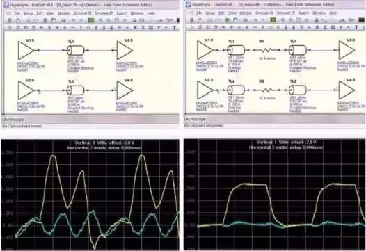
Figure 2: Elimination of signal quality and crosstalk problems using signal integrity analysis and design space exploration.
These same simulations can be run to determine the transmission time when the signal passes through the board. Board timing is an important part of system timing and is affected by the length of the line, its propagation speed as it passes through the board, and the shape of the waveform in the receiver. Since the shape of the waveform determines the time that the received signal crosses the logic threshold, it is very important for timing. These simulations typically drive changes in trace length constraints.
Another signal integrity simulation that typically runs is crosstalk. This involves multiple mutually coupled transmission lines. As the traces crowd into dense board designs, it is important to understand how much energy they are coupling to each other to eliminate errors caused by crosstalk. These simulations will drive the minimum spacing requirements between traces.
Power integrity simulation
In power integrity analysis, the main simulation types are DC voltage drop analysis, decoupling analysis, and noise analysis. DC voltage drop analysis includes analysis of complex traces and planar shapes on the PCB that can be used to determine how much voltage will be lost due to copper resistance. In addition, DC dropout analysis can be used to determine high current density regions. In fact, they can be co-simulated using a thermal simulator to see the thermal effects. Fortunately, the solution to the DC voltage drop problem is simple: add more metal. These additional metals may use wider and/or thicker traces and planar shapes, additional planes or additional vias.
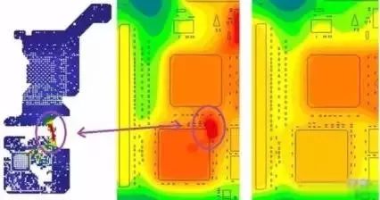
Figure 3: Current density and temperature plots showing "hot spots" in PI/thermal co-simulation
The decoupling analysis briefly discussed above is designed to minimize and minimize the impedance between the power supply and the ground at different IC locations on the board. Decoupling analysis typically drives changes in the value, type, and number of capacitors used in the PDN. Therefore, it requires a capacitor model that includes parasitic inductance and resistance. It also drives changes in capacitor mounting and/or board stack variations to meet low impedance requirements.
The type of noise analysis may vary. They can include noise from the IC power pins that propagate around the board and can be controlled by decoupling capacitors. Through noise analysis, it is possible to investigate how noise is coupled from one via to another, and the synchronous switching noise can be analyzed. In many cases, this noise is caused by signal switching (from 1 to 0 and from 0 to 1), so it is closely related to signal integrity. But in all cases, the ultimate goal of these power integrity analysis is to drive changes in the PDN: power/ground plane pairs, traces, capacitors, and vias.
Table 1. Differences between signal integrity and power integrity
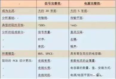
The PDN acts not only as a means of supplying current to the IC, but also as a return current path for the signal. A large amount of intersection between signal integrity and power integrity occurs in the vias. For a single-ended signal that passes through a via, the PDN acts as a return current path for that signal. A nearby via or capacitor provides a path for the return current to move from one plane to the next. Therefore, the PDN actually determines the impedance and delay characteristics of the single-ended via and is critical for accurate modeling of faster single-ended signals such as DDR3 and DDR4. Using this same SI/PI combined via model, the coupling from one via to the next via and the coupling of the signal through the via to the PDN can be analyzed.
As such, PDN is critical to minimize the noise that can be caused by multiple signal switching (commonly referred to as SSN). If the PDN impedance in the IC power pin is too high, when all the drivers switch at the same time, their switching current will generate a voltage that can be observed in the signal itself. This problem can be eliminated by designing an excellent low-impedance PDN using decoupling analysis. Fully simulate this problem to see the impact on the signal, requiring simultaneous signal integrity analysis and power integrity analysis. The SPICE model of the driver is traditionally used to perform such analysis, but the updated IBIS model also has a corresponding infrastructure to include PDN effects when looking for signal integrity.
Analysis of signal integrity and power integrity is critical to a successful high-speed digital design. They provide valuable insights into which design changes need to be made. In addition, as modeling methods and computing power improve, if both types of integrity can be simulated simultaneously, the actual behavior of the circuit, the real profit in the design, and how they achieve the best possible performance are clearly understood.
Several considerations for power integrity design
1. Power system noise margin analysis
Most chips give a normal operating voltage range, which is typically ±5%. Older regulator chips typically have an output voltage accuracy of ±2.5%, so the peak amplitude of the power supply noise should not exceed ±2.5%. Accuracy is conditional, including load conditions, operating temperature, etc., so there is a margin.
Power supply noise margin calculation
For example, the normal operating voltage range of the chip is between 3.13V and 3.47V, and the nominal output of the voltage regulator chip is 3.3V. After being mounted on the board, the regulator chip outputs 3.36V. Then the allowable voltage variation range is 3.47-3.36=0.11V=110mV. The output voltage of the regulator chip is ±1%, which is ±3.363*1%=±33.6mV. The power supply noise margin is 110-33.6=76.4mV.
2. How does the power supply noise produce?
First, the output of the regulated power supply chip itself is not constant and there will be some ripple.
Second, the regulated power supply cannot respond to the load in rapid response to rapid changes in current demand. The regulated power supply chip adjusts its output current by sensing the change in its output voltage, thereby adjusting the output voltage back to the rated output value.
Third, the voltage drop generated by the load transient current on the power path impedance and the ground path impedance, the parasitic inductance of the pin and the pad itself, and the transient current flowing through the path will inevitably cause a voltage drop, so the load chip power supply The voltage at the pin fluctuates as the transient current changes, which is the power supply noise generated by the impedance.
3, two explanations of capacitor decoupling
Capacitor decoupling is the main method to solve the power supply noise problem. This method is very effective in increasing the response speed of transient currents and reducing the impedance of the power distribution system.
3.1 From the perspective of energy storage to illustrate the principle of capacitor decoupling
When making a board, usually a lot of capacitors are placed around the load chip, and these capacitors act as a power supply decoupling. The principle can be illustrated in Figure 1.

When the load current is constant, its current is supplied by the regulated power supply section, that is, I0 in the figure, and the direction is as shown. At this time, the voltage across the capacitor is the same as the voltage across the load, and the current Ic is 0. The capacitor stores a considerable amount of charge at both ends, and the amount of charge is related to the capacitance. When the load transient current changes, the load chip needs to supply enough current in a very short time due to the extremely fast transistor level shifting speed inside the load chip. However, the regulated power supply cannot respond to changes in the load current very quickly. Therefore, the current I0 does not immediately meet the load transient current requirement, so the load chip voltage is reduced. However, since the capacitor voltage is the same as the load voltage, there is a voltage change across the capacitor. For a capacitor, a voltage change inevitably generates a current. At this time, the capacitor discharges to the load, and the current Ic is no longer zero, providing current to the load chip. As long as the capacitance C is large enough, only a small voltage change is required, and the capacitor can supply a large enough current to meet the load current requirement.
Equivalent to the capacitor pre-stored a part of the electrical energy, released when the load is needed, that is, the capacitor is the energy storage component. The existence of the storage capacitor allows the energy consumed by the load to be quickly replenished, thus ensuring that the voltage across the load does not change much. At this time, the capacitor is responsible for the role of the local power supply.
Understanding power supply decoupling from the perspective of energy storage is very intuitive and easy to understand, but it does not help much in circuit design. Understanding capacitor decoupling from the perspective of impedance allows us to follow the rules when designing circuits. In fact, the concept of impedance is used when deciding the decoupling capacitor of a power distribution system.
3.2 Understanding the decoupling principle from the perspective of impedance
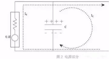
Remove the load chip from Figure 1, as shown in Figure 2. Looking from the AB point to the left, the regulated power supply and the capacitor decoupling system can be viewed as a composite power system. The characteristic of this power system is that no matter how the load transient current changes between the two points of AB, the voltage between the two points of AB can be kept basically stable, that is, the voltage change between the two points of AB is small.
We can use an equivalent power model to represent the composite power system above, as shown in Figure 3.
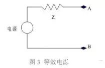
For this circuit you can write the following equation:

Our ultimate design goal is to maintain a small voltage variation between the two points of AB regardless of the change in load transient current between the two points. According to the above formula, this requirement is equivalent to the impedance Z of the power supply system being low enough. In Figure 2, we achieve this by decoupling capacitors, so from an equivalent point of view, it can be said that the decoupling capacitor reduces the impedance of the power system. On the other hand, from the perspective of circuit theory, the same conclusion can be drawn. Capacitors exhibit low impedance characteristics for AC signals, so adding capacitors actually reduces the AC impedance of the power system (1/jwc).
Understanding capacitor decoupling from the perspective of impedance can give us great convenience in designing a power distribution system. In fact, the most fundamental principle of power distribution system design is to minimize impedance. The most effective design method is produced under the guidance of this principle.
4, the characteristics of the actual capacitor
Proper use of capacitors for power supply decoupling requires an understanding of the frequency characteristics of the actual capacitors. Ideal capacitors do not exist in practice, which is why "capacitors are more than just capacitors" are often heard.
There are always some parasitic parameters in the actual capacitors. These parasitic parameters are not obvious at low frequencies, but at high frequencies, their importance may exceed the capacitance itself. Figure 4 shows the SPICE model of the actual capacitor. In the figure, ESR represents the equivalent series resistance, ESL represents the equivalent series inductance or parasitic inductance, and C is the ideal capacitance.
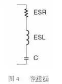
The equivalent series inductance (parasitic inductance) cannot be eliminated, and as long as the lead is present, there will be parasitic inductance. This can be easily understood from the viewpoint of the change of the magnetic field energy. When the current changes, the magnetic field energy changes, but the energy jump is impossible, and the inductance characteristic is exhibited. The parasitic inductance will delay the change of the capacitor current. The larger the inductance, the larger the capacitor charge and discharge impedance and the longer the reaction time.
The self-resonant frequency point is a dividing point that distinguishes whether the capacitance is capacitive or inductive. When the resonance frequency is higher than the resonant frequency, the “capacitance is no longer a capacitorâ€, so the decoupling effect will decrease.
The equivalent series inductance of a capacitor is related to the manufacturing process and package size. Usually, the capacitor of a small package has a lower equivalent series inductance, and the capacitance of a wide package has a lower equivalent series inductance than the capacitance of a narrow package.
Some large capacitors are placed on the board, usually tan or electrolytic capacitors. These capacitors have a very low ESL, but the ESR is very high, so the Q is very low and has a wide effective frequency range, making it ideal for board-level power supply filtering.
The higher the quality factor of the circuit, the higher the voltage across the inductor or capacitor than the applied voltage. The higher the Q value, the faster the current drops at a certain frequency offset, and the sharper the resonance curve. That is to say, the selectivity of the circuit is determined by the quality factor Q of the circuit, and the higher the Q value, the better the selectivity.
5, local decoupling design method
In order to ensure that the logic circuit can work normally, the level value indicating the logic state of the circuit must fall within a certain range. For example, for 3.3V logic, the high level is greater than 2V for logic 1, and the low level is less than 0.8V for logic 0.
Place the capacitor next to the device across the power and ground pins. Normally, the capacitor is charged and a portion of the charge is stored. The transient current required for such circuit switching is no longer provided by VCC, which is equivalent to a local small power supply. Therefore, the parasitic inductance of the power supply terminal and the ground terminal are bypassed, and the parasitic inductance does not flow current at this moment, and thus there is no induced voltage. Usually two or more capacitors are placed in parallel to reduce the series inductance of the capacitor itself, thereby reducing the impedance of the capacitor charging and discharging circuit.
Note: capacitor placement, mounting distance, mounting method, capacitor selection
Fan Motor,Blower Motor,Condenser Fan,Condenser Fan Motor
Wentelon Micro-Motor Co.,Ltd. , https://www.wentelon.com
